www.ti.com
ꢀꢁ ꢂ ꢃꢄ ꢅꢆ ꢇ
SLVS398D − JUNE 2001 − REVISED JULY 2003
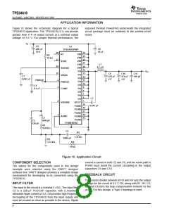
The only components that must tie directly to the power
ground plane are the input capacitor, the output capacitor,
the input voltage decoupling capacitor, and the PGND pins
of the TPS54610. The layout of the TPS54610 evaluation
module is representative of a recommended layout for a
4-layer board. Documentation for the TPS54610
evaluation module can be found on the Texas Instruments
web site under the TPS54610 product folder. See the
TPS54610 EVM user’s guide, TI literature number
SLVU054, and the application note, TI literature number
SLVA104.
OPERATING FREQUENCY
In the application circuit, the 350 kHz operation is selected
by leaving RT and SYNC open. Connecting a 180 kΩ to 68
kΩ resistor between RT (pin 28) and analog ground can be
used to set the switching frequency to 280 kHz to 700 kHz.
To calculate the RT resistor, use the equation below:
500 kHz
Switching Frequency
R +
100 [kW]
(1)
OUTPUT FILTER
LAYOUT CONSIDERATIONS FOR THERMAL
PERFORMANCE
The output filter is composed of a 4.7-µH inductor and two
470-µF capacitors. The inductor is a low dc resistance (12
mΩ) type, Coiltronics UP3B−4R7. The capacitors used
are 4 V POSCAP types with a maximum ESR of 0.040 Ω.
The feedback loop is compensated so that the unity gain
frequency is approximately 25 kHz.
For operation at full rated load current, the analog ground
plane must provide an adequate heat dissipating area. A
3-inch by 3-inch plane of 1 ounce copper is recommended,
though not mandatory, depending on ambient temperature
and airflow. Most applications have larger areas of internal
ground plane available, and the PowerPAD must be
connected to the largest area available. Additional areas
on the top or bottom layers also help dissipate heat, and
any area available must be used when 6 A or greater
operation is desired. Connection from the exposed area of
the PowerPAD to the analog ground plane layer must be
made using 0.013 inch diameter vias to avoid solder
wicking through the vias. Eight vias must be in the
PowerPAD area with four additional vias located under the
device package. The size of the vias under the package,
but not in the exposed thermal pad area, can be increased
to 0.018. Additional vias beyond the twelve recommended
that enhance thermal performance must be included in
areas not under the device package.
GROUNDING AND POWERPAD LAYOUT
The TPS54610 has two internal grounds (analog and
power). Inside the TPS54610, the analog ground ties to all
of the noise sensitive signals, while the power ground ties
to the noisier power signals. The PowerPAD must be tied
directly to AGND. Noise injected between the two grounds
can degrade the performance of the TPS54610,
particularly at higher output currents. However, ground
noise on an analog ground plane can also cause problems
with some of the control and bias signals. Therefore,
separate analog and power ground planes are
recommended. These two planes must tie together
directly at the IC to reduce noise between the two grounds.
Minimum Recommended Thermal Vias: 8 x 0.013 Diameter Inside
Powerpad Area 4 x 0.018 Diameter Under Device as Shown.
Additional 0.018 Diameter Vias May Be Used if Top Side Analog Ground
Area Is Extended.
Ø0.0130
8 PL
4 PL Ø0.0180
Connect Pin 1 to Analog Ground Plane
in This Area for Optimum Performance
0.0150
0.06
0.0339
0.0650
0.0500
0.3820 0.3478
0.2090
0.0256
0.0500
0.0500
0.0650
0.0339
Minimum Recommended Exposed
Copper Area for Powerpad. 5mm
Stencils May Require 10 Percent
0.1700
Larger Area
0.1340
0.0630
Minimum Recommended Top
Side Analog Ground Area
0.0400
Figure 11. Recommended Land Pattern for 28-Pin PWP PowerPAD
9

 TI [ TEXAS INSTRUMENTS ]