TPS54531
www.ti.com
SLVSBI5 –MAY 2013
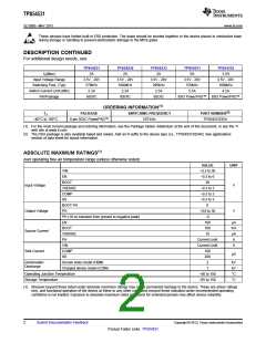
PACKAGE DISSIPATION RATINGS(1) (2) (3)
THERMAL IMPEDANCE
JUNCTION TO AMBIENT
PSEUDO THERMAL IMPEDANCE
PACKAGE
JUNCTION TO TOP
SOIC8 PowerPAD™
50°C/W
5°C/W
(1) Maximum power dissipation may be limited by overcurrent protection
(2) Power rating at a specific ambient temperature TA should be determined with a junction temperature of 150°C. This is the point where
distortion starts to substantially increase. Thermal management of the PCB should strive to keep the junction temperature at or below
150°C for best performance and long-term reliability. See power dissipation estimate in application section of this data sheet for more
information.
(3) Test board conditions:
(a) 2 inches x 1.5 inches, 2 layers, thickness: 0.062 inch
(b) 2-ounce copper traces located on the top and bottom of the PCB
(c) 6 thermal vias located under the device package
RECOMMENDED OPERATING CONDITIONS
over operating free-air temperature range (unless otherwise noted)
MIN
3.5
TYP
MAX UNIT
Operating Input Voltage on (VIN pin)
Operating junction temperature, TJ
28
V
–40
150
°C
ELECTRICAL CHARACTERISTICS
TJ = –40°C to 150°C, VIN = 3.5V to 28V (unless otherwise noted)
DESCRIPTION
TEST CONDITIONS
MIN
TYP
MAX UNIT
SUPPLY VOLTAGE (VIN PIN)
Internal undervoltage lockout threshold
Shutdown supply current
Operating – non switching supply current
ENABLE AND UVLO (EN PIN)
Enable threshold
Rising and Falling
3.5
4
V
EN = 0V, VIN = 12V, –40°C to 85°C
VSENSE = 0.85 V
1
μA
μA
110
190
Rising and Falling
1.25
-1
1.35
V
Input current
Enable threshold – 50 mV
Enable threshold + 50 mV
μA
μA
Input current
-4
VOLTAGE REFERENCE
Voltage reference
0.772
0.8 0.828
V
HIGH-SIDE MOSFET
BOOT-PH = 3 V, VIN = 3.5 V
BOOT-PH = 6 V, VIN = 12 V
115
80
200
150
mΩ
On resistance
ERROR AMPLIFIER
Error amplifier transconductance (gm)
Error amplifier DC gain(1)
Error amplifier unity gain bandwidth(1)
Error amplifier source/sink current
Switch current to COMP transconductance(1)
SWITCHING FREQUENCY
–2 μA < I(COMP) < 2 μA, V(COMP) = 1 V
VSENSE = 0.8 V
92
800
2.7
±7
μmhos
V/V
5 pF capacitance from COMP to GND pins
V(COMP) = 1 V, 100 mV overdrive
VIN = 12 V
MHz
μA
20
A/V
Switching Frequency
VIN = 12V, 25°C
VIN = 12V, 25°C
BOOT-PH = 6 V
456
570
105
684
130
kHz
ns
Minimum controllable on time
Maximum controllable duty ratio(1)
PULSE SKIPPING ECO-MODE™
Pulse skipping Eco-mode™ switch current threshold
CURRENT LIMIT
90%
93%
160
mA
A
Current limit threshold
VIN = 12 V
6.3
10.5
(1) Specified by design
Copyright © 2013, Texas Instruments Incorporated
Submit Documentation Feedback
3
Product Folder Links: TPS54531

 TI [ TEXAS INSTRUMENTS ]