TPS51211
SLUSAA7 –NOVEMBER 2010
www.ti.com
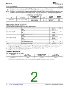
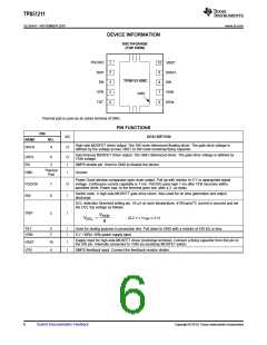
DEVICE INFORMATION
DSC PACKAGE
(TOP VIEW)
PGOOD
TRIP
EN
1
2
3
4
5
10 VBST
9
8
7
6
DRVH
SW
TPS51211DSC
VFB
V5IN
DRVL
GND
TST
Thermal pad is used as an active terminal of GND.
PIN FUNCTIONS
PIN
I/O
DESCRIPTION
NAME
NO.
High-side MOSFET driver output. The SW node referenced floating driver. The gate drive voltage is
defined by the voltage across VBST to SW node bootstrap flying capacitor
DRVH
9
O
Synchronous MOSFET driver output. The GND referenced driver. The gate drive voltage is defined by
V5IN voltage.
DRVL
EN
6
3
O
I
SMPS enable pin. Short to GND to disable the device.
Thermal
Pad
GND
I
Ground
Power Good window comparator open drain output. Pull up with resistor to 5 V or appropriate signal
voltage. Continuous current capability is 1 mA. PGOOD goes high 1 ms after VFB becomes within
specified limits. Power bad, or the terminal goes low, after a 2- ms delay.
PGOOD
SW
1
8
O
I
Switch node. A high-side MOSFET gate drive return. Also used for on time generation and output
discharge.
OCL detection threshold setting pin. 10 mA at room temperature, 4700 ppm/°C current is sourced and set
the OCL trip voltage as follows.
TRIP
2
I
V
TRIP
V
=
(0.2 V ≤ VTRIP ≤ 3 V)
OCL
8
TST
5
7
I
I
Used for testing purpose in production line. Pull down to GND with a resistor of 470 kΩ or less.
V5IN
5-V +30%/–10% power supply input.
Supply input for high-side MOSFET driver (bootstrap terminal). Connect a flying capacitor from this pin to
the SW pin. Internally connected to V5IN via bootstrap MOSFET switch.
VBST
VFB
10
4
I
I
SMPS feedback input. Connect the feedback resistor divider.
6
Submit Documentation Feedback
Copyright © 2010, Texas Instruments Incorporated

 TI [ TEXAS INSTRUMENTS ]