TPS51211
SLUSAA7 –NOVEMBER 2010
www.ti.com
This integrated circuit can be damaged by ESD. Texas Instruments recommends that all integrated circuits be handled with
appropriate precautions. Failure to observe proper handling and installation procedures can cause damage.
ESD damage can range from subtle performance degradation to complete device failure. Precision integrated circuits may be more
susceptible to damage because very small parametric changes could cause the device not to meet its published specifications.
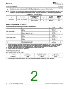
ORDERING INFORMATION
ORDERING DEVICE
NUMBER
OUTPUT
SUPPLY
MINIMUM
QUANTITY
TA
PACKAGE
PINS
TPS51211DSCR
TPS51211DSCT
10
10
Tape and reel
Mini reel
3000
250
–40°C to 85°C
Plastic SON PowerPAD
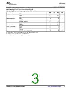
ABSOLUTE MAXIMUM RATINGS(1)
over operating free-air temperature range (unless otherwise noted)
VALUE
UNIT
VBST
VBST(3)
–0.3 to 37
–0.3 to 7
–5 to 30
–0.3 to 7
–5 to 37
–0.3 to 7
–0.5 to 7
–0.3 to 7
150
Input voltage range(2)
SW
V
V5IN, EN, TRIP, VFB, TST
DRVH
DRVH(3)
Output voltage range(2)
DRVL
V
PGOOD
TJ
Junction temperature range
Storage temperature range
°C
°C
TSTG
–55 to 150
(1) Stresses beyond those listed under absolute maximum ratings may cause permanent damage to the device. These are stress ratings
only and functional operation of the device at these or any other conditions beyond those indicated under recommended operating
conditions is not implied. Exposure to absolute-maximum-rated conditions for extended periods may affect device reliability.
(2) All voltage values are with respect to the network ground terminal unless otherwise noted.
(3) Voltage values are with respect to the SW terminal.
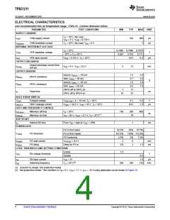
DISSIPATION RATINGS
2-oz. trace and copper pad with solder.
PACKAGE
TA < 25°C
POWER RATING
DERATING FACTOR
ABOVE TA = 25°C
TA = 85°C
POWER RATING
10-pin DSC(1)
1.54 W
15 mW/°C
0.62 W
(1) Enhanced thermal conductance by thermal vias is used beneath thermal pad as shown in Land Pattern information.
2
Submit Documentation Feedback
Copyright © 2010, Texas Instruments Incorporated

 TI [ TEXAS INSTRUMENTS ]