TPS51640A, TPS59640, TPS59641
www.ti.com
SLUSAQ2 –JANUARY 2012
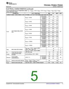
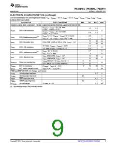
ELECTRICAL CHARACTERISTICS (continued)
over recommended free-air temperature range, VV5 = VV5DRV = 5.0 V; VV3R3 = 3.3 V; VxGFB = VPGND = VGND, VxVFB = VCORE
(Unless otherwise noted)
PARAMETER
TEST CONDITIONS
MIN
TYP
MAX
UNIT
DRIVERS: HIGH-SIDE, LOW-SIDE, CROSS CONDUCTION PREVENTION AND BOOST RECTIFIER
(VCBSTx – VCSWx) = 5 V, ‘HI’ state,
(VVBST – VVDRVH) = 0.25 V
1.2
0.8
2.5
2.5
RDRVH
DRVH ON resistance
Ω
(VCBSTx – VCSWx) = 5 V, ‘LO’ state,
(VDRVH – VLL) = 0.25 V
VCDHx = 2.5 V, (VCBSTx – VCSWx) = 5 V, Source
VCDHx = 2.5 V, (VCBSTx – VCSWx) = 5 V, Sink
2.2
2.2
15
15
0.9
0.4
2.7
6
A
A
IDRVH
DRVH sink/source current(3)
DRVH transition time
40
40
2
ns
ns
tDRVH
CDHx 10% to 90% or 90% to 10%, CCDHx = 3 nF
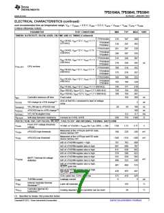
‘HI’ State, (VV5DRV – VVDRVL) = 0.25 V
‘LO’ State, (VVDRVL – VPGND)= 0.2 V
VCDLx = 2.5 V, Source
RDRVL
DRVL ON resistance
Ω
1
A
A
IDRVL
DRVL sink/source current(3)
DRVL transition time
VCDLx = 2.5 V, Sink
VCDLx 90% to 10%, CCDLx = 3 nF
VCDLx 10% to 90%, CCDLx = 3 nF
VCSWx falls to 1 V to VCDLx rises to 1 V
CDLx falls to 1 V to CDHx rises to 1 V
(VV5DRV – VVBST), IF = 5 mA
15
15
25
25
10
0.1
40
40
tDRVL
ns
ns
13
13
5
tNONOVLP
Driver non overlap time
RDS(on)
IBSTLK
BST on-resistance
20
1
Ω
BST switch leakage current
VVBST = 34 V, VCSWx=28 V
µA
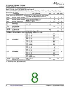
PWM and SKIP OUTPUT: I/O Voltage and Current
VPWML
VPWMH
VSKIPL
xPWMy output low level
xPWMy output high level
SKIP output low level
xSKIP output high level
xPWM leakage
0.7
0.7
0.1
V
V
4.2
4.2
V
VSKIPH
VPW(leak)
V
Tri-state, V = 5 V
µA
(3) Specified by design. Not production tested.
Copyright © 2012, Texas Instruments Incorporated
Submit Documentation Feedback
9

 TI [ TEXAS INSTRUMENTS ]