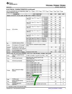
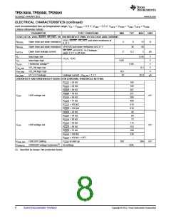
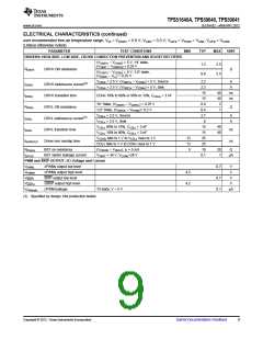
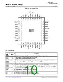
TPS51640A, TPS59640, TPS59641
www.ti.com
SLUSAQ2 –JANUARY 2012
PIN
I/O
DESCRIPTION
Voltage divider to VREF. A resistor to GND sets the operating frequency of the CPU converter. The voltage level
NAME
NO.
CF-IMAX
13
I
sets the maximum operating current of the CPU converter. The IMAX value is an 8-bit A/D where VIMAX = VREF
IMAX / 255. Both are latched at start-up.
×
Voltage sense return tied for the CPU converter. Tie to GND with a 10-Ω resistor to close feedback when the
microprocessor is not in the socket.
CGFB
12
3
I
Analog current monitor output for the CPU converter. VCIMON = ΣVCS × ACS × (1 + RCIMON/RCOCP). Connect a
220-nF capacitor to GND for stability.
CIMON
COCP-I
O
Resistor to GND (RCOCP) selects 1 of 8 OCP levels (per phase, latched at start-up) of the CPU converter. Also,
voltage divider to CIMON. Resistor ratio sets the IMON gain (see CIMON pin description).
2
I
CPGOOD
CSW1
17
45
40
36
O
IMVP-7_PWRGD output for the CPU converter. Open-drain.
I/O Top N-channel FET gate drive return for CPU phase 1.
I/O Top N-channel FET gate drive return for CPU phase 2.
CSW2
CPWM3
O
PWM control for the external driver, 5V logic level.
Skip mode control of the external driver for the CPU converter. A logic HI = FCCM, LO = SKIP. R to GND selects
1 of 8 OSR/USR levels. 0.1 V < VCSKIP < 0.3 V at start-up turns OSR off.
CSKIP
35
1
O
Thermal sensor connection for the CPU converter. A resistor connected to VREF forms a divider with an NTC
thermistor connected to GND.
CTHERM
CVFB
I/O
I
Voltage sense line tied directly to VCORE of the CPU converter. Tie to VCORE with a 10-Ω resistor to close
feedback when µP is not in the socket. The soft-stop transistor is on this pin
11
Negative current sense input for the GPU converter. Connect to the most negative node of current sense resistor
or inductor DCR sense network. GCSN has a secondary OVP comparator and includes the soft-stop pull-down
transistor.
GCSN
28
I
Positive current sense input for the GPU converter. Connect to the most positive node of current sense resistor
or inductor DCR sense network. Tie to V3R3 to disable the GPU converter.
GCSP
29
27
25
24
I
O
I
GCOMP
GGFB
Output of gM error amplifier for the GPU converter. A resistor to VREF sets the droop gain.
Voltage sense return tied for the GPU converter. Tie to GND with a 10-Ω resistor to close feedback when the
microprocessor is not in the socket.
I
Voltage divider to VREF. R to GND sets the operating frequency of the GPU converter. The voltage level sets
GF-IMAX
the maximum operating current of the GPU converter. The IMAX value is an 8-bit A/D where VIMAX = VREF
IMAX / 255. Both are latched at start-up.
×
30
31
O
I
Analog current monitor output for the GPU converter. VGIMON = VISENSE × (1 + RGIMON/RGOCP). Connect a
220-nF capacitor to GND for stability.
GIMON
GOCP-I
Voltage divider to GIMON. Resistor ratio sets the IMON gain (see GIMON pin). Resistor to GND (RGOCP) selects
1 of 8 OCP levels (per phase, latched at start-up) of the GPU converter.
GPGOOD
GPWM
23
34
33
O
O
O
IMVP-7_PWRGD output for the GPU converter. Open-drain.
PWM control for the external driver, 5-V logic level.
Skip mode control of the external driver for the GPU converter, 5-V logic level. Logic HI = FCCM, LO = SKIP. R
to GND selects 1 of 8 OSR/USR levels. 0.1 V < VGSKIP< 0.3 V at start-up turns OSR off.
GSKIP
32
26
I/O Thermal sensor input for the GPU converter. A resistor connected to VREF forms a divider with an NTC
thermistor connected to GND.
GTHERM
I
Voltage sense line tied directly to VGFX of the GPU converter. Tie to VGFX with a 10-Ω resistor to close feedback
GVFB
when the microprocessor is not in the socket. The soft-stop transistor is on this pin
PGND
SLEWA
42
22
–
Synchronous N-channel FET gate drive return.
I
The voltage at start-up sets 1 of 7 slew rates for both converters. The SLOW rate is SLEWRATE/4. Soft-start
and soft-stop rates are SLEWRATE/8. This value is latched at start-up. Tie to GND to disable SCLK timer.
48
43
I
I
5-V power input for analog circuits; connect through resistor to 5-V plane and bypass to GND with ≥1 µF ceramic
capacitor
V5
Power input for the gate drivers; connected with an external resistor to V5F; decouple with a ≥2.2 µF ceramic
capacitor.
V5DRV
V3R3
15
37
I
I
3.3-V power input; bypass to GND with ≥1 µF ceramic cap.
Provides VBAT information to the on-time circuits for both converters. A 10-kΩ series resistor protects the
adjacent pins from inadvertent shorts due to solder bridges or mis-probing during test.
VBAT
VCLK
VDIO
VREF
18
20
14
I
SVID clock. 1-V logic level.
I/O SVID digital I/O line. 1-V logic level.
1.7-V, 500-µA reference. Bypass to GND with a 0.22-µF ceramic capacitor.
O
Copyright © 2012, Texas Instruments Incorporated
Submit Documentation Feedback
11

 TI [ TEXAS INSTRUMENTS ]