TPS51640A, TPS59640, TPS59641
SLUSAQ2 –JANUARY 2012
www.ti.com
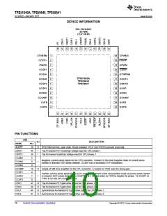
DEVICE INFORMATION
RSL PACKAGE
48 PINS
(TOP VIEW)
1
2
36
CTHERM
COCP-I
CIMON
CCSP1
CCSN1
CCSN2
CCSP2
CCSP3
CCSN3
CCOMP
CVFB
CPWM3
35 CSKIP
3
34
33
32
31
30
29
28
27
26
25
GPWM
GSKIP
GTHERM
GOCP-I
GIMON
GCSP
4
5
TPS51640A
TPS59640
TPS59641
6
7
8
9
GCSN
10
11
12
GCOMP
GVFB
CGFB
GGFB
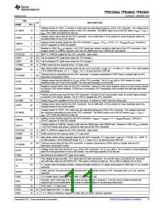
PIN FUNCTIONS
PIN
I/O
DESCRIPTION
NAME
NO.
19
46
39
5
ALERT
CBST1
CBST2
CCSN1
CCSN2
CCSN3
O
I
SVID interrupt line, open drain. Route between VCLK and VDIO to prevent cross-talk.
Top N-channel FET bootstrap voltage input for CPU phase 1.
I
Top N-channel bootstrap voltage input for CPU phase 2.
Negative current sense inputs for the CPU converter. Connect to the most negative node of current sense
resistor or inductor DCR sense network. CCSN1 has a secondary OVP comparator.
6
I
O
I
9
CCOMP
CCSP1
CCSP2
CCSP3
CDH1
10
4
Output of GM error amplifier for the CPU converter. A resistor to VREF sets the droop gain.
Positive current sense inputs for the CPU converter. Connect to the most positive node of current sense resistor
or inductor DCR sense network. Tie CCSP3, 2 or 1 (in that order) to V3R3 to disable the phase. Tie CCSP1 to
V3R3 to run the GPU converter only.
7
8
47
38
44
41
O
O
O
O
Top N-channel FET gate drive output for CPU phase 1.
Top N-channel FET gate drive output for CPU phase 2.
Synchronous N-channel FET gate drive output for CPU phase 1.
Synchronous N-channel FET gate drive output for CPU phase 2.
CDH2
CDL1
CDL2
10
Submit Documentation Feedback
Copyright © 2012, Texas Instruments Incorporated

 TI [ TEXAS INSTRUMENTS ]