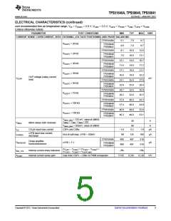
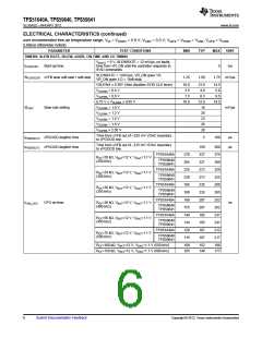
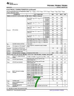
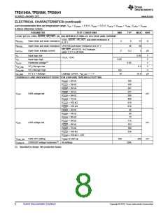
TPS51640A, TPS59640, TPS59641
SLUSAQ2 –JANUARY 2012
www.ti.com
These devices have limited built-in ESD protection. The leads should be shorted together or the device placed in conductive foam
during storage or handling to prevent electrostatic damage to the MOS gates.
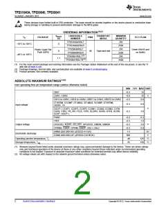
ORDERING INFORMATION(1)(2)
VBOOT
(V)
ORDERABLE
NUMBER
TRANSPORT
MEDIA
MINIMUM
QUANTITY
TA
PACKAGE
PINS
ECO PLAN
TPS51640ARSLT
TPS51640ARSLR
TPS59640RSLT
250
2500
250
–10°C to 105°C
0
0
Green (RoHS and
no Sb/Br)
Plastic Quad Flat
Pack (QFN)
48
Tape-and-reel
TPS59640RSLR
TPS59641RSLT(3)
TPS59641RSLTR(3)
2500
250
–40°C to 105°C
1.1
2500
(1) For the most current package and ordering information see the Package Option Addendum at the end of this document, or see the TI
web site at www.ti.com.
(2) Package drawings, thermal data, and symbolization are available at www.ti.com/packaging.
(3) Product preview. Not currently available.
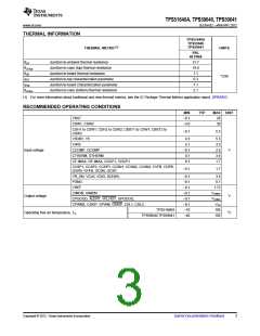
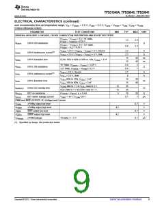
ABSOLUTE MAXIMUM RATINGS(1)(2)
over operating free-air temperature range (unless otherwise noted)
MIN TYP MAX UNIT
VBAT
–0.3
–6.0
–0.3
32
32
CSW1, CSW2
V
CDH1 to CSW1; CDH2 to CSW2; CBST1 to CSW1; CBST2 to CSW2
6.0
CTHERM, CCOMP, CF-IMAX, GF-IMAX, GCOMP, GTHERM,
V5DRV, V5
–0.3
6.0
Input voltage
V
COCP-I, CCSP1, CCSP2, CCSP3, CCSN1, CCSN2, CCSN3, CVFB,
CGFB, V3R3, VR_ON, VCLK, VDIO, SLEWA, GGFB, GVFB, GCSN,
GCSP, GOCP-I,
–0.3
3.6
PGND
–0.3
–0.3
–0.3
–0.3
1.5
0.3
1.8
3.6
6.0
VREF
Output voltage
CPGOOD, ALERT, VR_HOT, GPGOOD, CIMON, GIMON
CPWM3, CSKIP, GPWM, GSKIP, CDL1, CDL2
(HBM) QSS 009-105 (JESD22-A114A)
(CDM) QSS 009-147 (JESD22-C101B.01)
V
kV
V
Electrotatic discharge
500
-40
Operating junction temperature, TJ
Storage temperature, Tstg
125 °C
150 °C
-55
(1) Stresses beyond those listed under absolute maximum ratings may cause permanent damage to the device. These are stress ratings
only and functional operation of the device at these or any other conditions beyond those indicated under recommended operating
conditions is not implied. Exposure to absolute-maximum-rated conditions for extended periods may affect device reliability.
(2) All voltage values are with respect to the network ground terminal unless otherwise noted.
2
Submit Documentation Feedback
Copyright © 2012, Texas Instruments Incorporated

 TI [ TEXAS INSTRUMENTS ]