PDF
最近搜索
热门搜索
发布采购

| 型号: | TPS51285A |
| PDF下载: | 下载PDF文件 查看货源 |
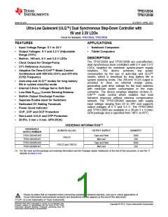
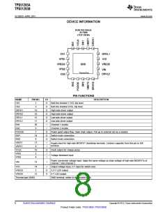
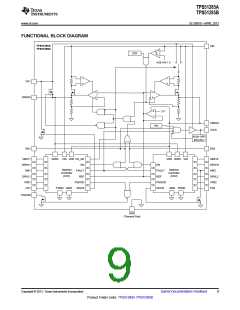
| 内容描述: | 超低静态( ULQâ ?? ¢ )双路同步降压型控制器, 5V和3.3V的LDO [Ultra-Low Quiescent (ULQâ¢) Dual Synchronous Step-Down Controller with 5V and 3.3V LDOs] |
| 分类和应用: | 控制器 |
| 文件页数/大小: | 32 页 / 1375 K |
| 品牌: |  TI [ TEXAS INSTRUMENTS ] TI [ TEXAS INSTRUMENTS ] |
专业IC领域供求交易平台:提供全面的IC Datasheet资料和资讯,Datasheet 1000万数据,IC品牌1000多家。