TPS43060
TPS43061
www.ti.com
SLVSBP4A –DECEMBER 2012–REVISED DECEMBER 2012
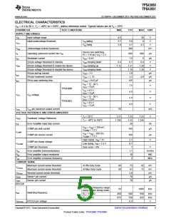
ELECTRICAL CHARACTERISTICS
VIN = 4.5 to 38 V, TJ = -40ºC to +150ºC, unless otherwise noted. Typical values are at TA = 25ºC
PARAMETER
TEST CONDITIONS
MIN
TYP
MAX
UNIT
SUPPLY AND ENABLE
VIN
Input voltage range
4.5
3.7
3.9
38
4
V
V
Input undervoltage threshold
VIN falling
VIN rising
3.9
4.1
VUV
4.3
V
Vhys
IQ
Undervoltage lockout hysteresis
200
mV
Device non-switching,
RT = 115 kΩ, VFB = 2 V
Operating quiescent current into VIN
600
800
µA
ISD
Shutdown current
VEN = 0.4V
1.5
0.7
5
0.9
µA
V
EN pin voltage threshold to standby
EN pin voltage threshold to enable the device
EN pin voltage threshold to disable the device
EN pin pull-up current
VEN ramping down
VEN ramping up
VEN ramping down
VEN = 1 V
0.4
1.12
1
VEN
1.21
1.14
1.8
1.29
1.28
V
V
µA
µA
µs
IEN
tEN
EN pin hysteresis current
VEN = 1. 3V
3.2
4.6
EN to start switching time
CVCC = 0.47 µF
125
VIN = 12 - 38 V,
IVCC = 0 µA
7.5
4.5
5.5
4.5
V
V
V
TPS43060
VIN = 4.5 V,
IVCC = 0 µA
VCC
VCC voltage
VIN = 12 - 38 V,
IVCC = 0 µA
TPS43061
VIN = 4.5 V,
IVCC = 0 µA
V
IVCC
VCC pin maximum output current
50
mA
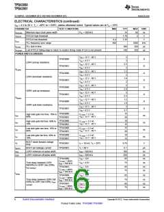
VOLTAGE REFERENCE AND ERROR AMPLIFIER
TJ = 25°C
1.21
1.22
1.22
20
1.23
V
VREF
IFB
Feedback Voltage Reference
TJ = -40°C to 150°C
1.195
1.244
Error Amplifier input bias current
COMP pin sink current
nA
µA
VFB = VREF + 250 mV,
VCOMP = 1.5 V
160
160
ICOMP
VFB = VREF - 250 mV,
VCOMP = 1.5 V
COMP pin source current
COMP pin clamp voltage
µA
V
High clamp, VFB = 1V
Low clamp, VFB = 1.5 V
Duty cycle = 0%
2.1
0.7
1
VCLAMP
COMP pin threshold
V
Gea
Rea
Fea
Error amplifier transconductance
Error amplifier output resistance
Error amplifier crossover frequency
1.1
10
2
m-mho
MΩ
MHz
CURRENT SENSE
Maximum current sense threshold
At 0% Duty Cycle
At Max Duty Cycle
64
50
73
61
3.8
70
70
82
72
mV
mV
mV
µA
VCSmax
Maximum current sense threshold
Reverse current sense threshold
Sense+ pin current
VRCsns
ISNS+
ISNS-
Sense- pin current
µA
RT/CLK
Operating frequency range
using resistor timing mode
50
1000
kHz
fSW
Switching frequency
RT/CLK pin voltage
RT = 115 kΩ
RT = 75 kΩ
450
675
500
750
0.5
550
825
kHz
kHz
V
VRT/CLK
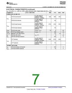
Copyright © 2012, Texas Instruments Incorporated
Submit Documentation Feedback
5
Product Folder Links: TPS43060 TPS43061

 TI [ TEXAS INSTRUMENTS ]