TPS43060
TPS43061
www.ti.com
SLVSBP4A –DECEMBER 2012–REVISED DECEMBER 2012
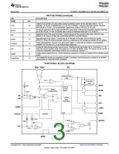
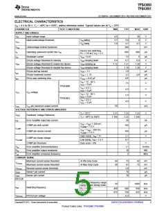
PIN FUNCTIONS (continued)
PIN
DESCRIPTION
NAME
NO.
Output of an internal LDO and power supply for internal control circuits and gate drivers. VCC is
typically 7.5V for the TPS43060 and 5.5 V for the TPS43061. Connect a low ESR ceramic capacitor
from this pin to PGND. The recommended capacitance range is from 0.47 µF to 10µF.
VCC
10
Bootstrap capacitor node for high-side MOSFET gate driver. Connect the bootstrap capacitor from this
pin to the SW pin. For the TPS43060, also connect a bootstrap diode from VCC to BOOT.
BOOT
SW
11
12
13
14
Switching node of the boost converter. Connect this pin to the junction of the drain of the low side
MOSFET, the source of high side synchronous MOSFET and the inductor.
High side gate driver output. Connect this pin to the gate of the high side synchronous rectifier
MOSFET. When VIN bias is removed, this pin is connected to SW through an internal 200 kΩ resistor.
HDRV
PGOOD
Power good indicator. This pin is an open-drain output. A 10 kΩ pull-up resistor is recommended
between PGOOD and VCC or an external logic supply pin.
Enable pin with internal pull-up current source. Floating this pin will enable the IC. Pull below 1.2 V to
enter low current standby mode. Pull below 0.4 V to enter shutdown mode. The EN pin can be used to
implement adjustable undervoltage lockout (UVLO) using two resistors.
EN
15
Analog signal ground of the IC. AGND should be connected to PGND at a single point on printed circuit
board.
AGND
16
17
The PowerPAD should be connected to AGND. If possible, use thermal vias to connect to an internal
ground plane for improved power dissipation.
PowerPAD
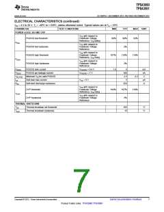
FUNCTIONAL BLOCK DIAGRAM
VIN
ISNS- ISNS+
5.5V or 7.5V
LDO
ILIM
TPS43061
only
BOOT
HDRV
5µA
Reverse
Current
Detect
Slope
Compensation
1.22V
SS
SW
R
S
LOGIC
and
CONTROL
FB
VCC
COMP
LDRV
OVP
PGND
OSC/PLL
RT/CLK
3.2µA
1.342V
PGOOD
1.8µA
O
FB
EN
1.21V
1.098V
AGND
Copyright © 2012, Texas Instruments Incorporated
Submit Documentation Feedback
3
Product Folder Links: TPS43060 TPS43061

 TI [ TEXAS INSTRUMENTS ]