TPS43060
TPS43061
SLVSBP4A –DECEMBER 2012–REVISED DECEMBER 2012
www.ti.com
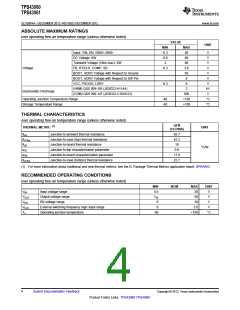
These devices have limited built-in ESD protection. The leads should be shorted together or the device placed in conductive foam
during storage or handling to prevent electrostatic damage to the MOS gates.
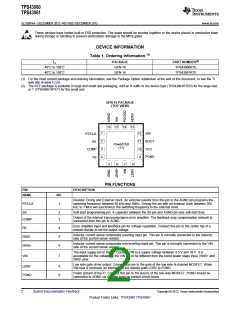
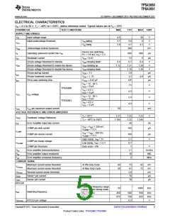
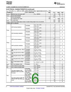
DEVICE INFORMATION
(1)
Table 1. Ordering Information
TJ
PACKAGE
QFN-16
PART NUMBER(2)
TPS43060RTE
TPS43061RTE
-40˚C to 150˚C
-40˚C to 150˚C
QFN-16
(1) For the most current package and ordering information, see the Package Option Addendum at the end of this document, or see the TI
web site at www.ti.com.
(2) The RTE package is available in large and small reel packaging. Add an R suffix to the device type (TPS43061RTER) for the large reel,
or T (TPS43061RTET) for the small reel.
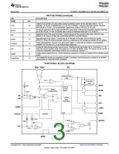
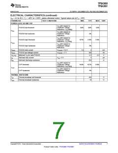
QFN-16 PACKAGE
(TOP VIEW)
16 15 14 13
1
2
3
4
12 SW
RT/CLK
SS
BOOT
11
10
9
PowerPAD
(17)
VCC
COMP
FB
PGND
5
6
7
8
PIN FUNCTIONS
PIN
DESCRIPTION
NAME
NO.
Resistor Timing and External Clock. An external resistor from this pin to the AGND pin programs the
switching frequency between 50 kHz and 1MHz. Driving the pin with an external clock between 300
kHz to 1 MHz will synchronize the switching frequency to the external clock.
RT/CLK
1
SS
2
3
Soft-start programming pin. A capacitor between the SS pin and AGND pin sets soft-start time.
Output of the internal transconductance error amplifier. The feedback loop compensation network is
connected from this pin to AGND.
COMP
Error amplifier input and feedback pin for voltage regulation. Connect this pin to the center tap of a
resistor divider to set the output voltage.
FB
4
5
6
Inductor current sense comparator inverting input pin. This pin is normally connected to the inductor
side of the current sense resistor.
ISNS-
ISNS+
Inductor current sense comparator non-inverting input pin. This pin is normally connected to the VIN
side of the current sense resistor.
The input supply pin to the IC. Connect VIN to a supply voltage between 4.5 V and 38 V. It is
acceptable for the voltage on the VIN pin to be different from the boost power stage input, ISNS+ and
ISNS- pins.
VIN
7
Low side gate driver output. Connect this pin to the gate of the low side N-channel MOSFET. When
VIN bias is removed, an internal 200 kΩ resistor pulls LDRV to PGND.
LDRV
PGND
8
9
Power ground of the IC. Connect this pin to the source of the low-side MOSFET. PGND should be
connected to AGND via a single point on printed circuit board.
2
Submit Documentation Feedback
Copyright © 2012, Texas Instruments Incorporated
Product Folder Links: TPS43060 TPS43061

 TI [ TEXAS INSTRUMENTS ]