TPS40200-Q1
www.ti.com
SLUS739D –SEPTEMBER 2006–REVISED JULY 2011
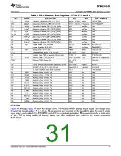
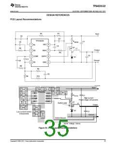
DESIGN REFERENCES
PCB Layout Recommendations
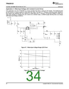
R3
R1
C3
Input
C5
TPS40200
VDD
RSENSE
C1
C6
1
2
3
4
8
RC
SS
C4
Q1
R5
L1
Output
Ground
ISEN
GDRV
GND
7
R4
C2
COMP
FB
6
5
D1
C7
C8
R8
R9
C9
R6
R10
UDG-07045
Input
R1
C4
R3
TPS40200
C3
C5
C6
R5
R4
RC
SS
VDD
ISEN
GDRV
GND
RSENSE
C1
High current
Power stage components
COMP
FB
Q1
Switch node
L1
Output
R6
R9
R8
D1
C2
Low current Control
Components
R10
Ground
Kelvin Ground
Kelvin Voltage Sense
Figure 53. PCB Layout Recommendations
Copyright © 2006–2011, Texas Instruments Incorporated
35

 TI [ TEXAS INSTRUMENTS ]