TPS40200-Q1
SLUS739D –SEPTEMBER 2006–REVISED JULY 2011
www.ti.com
Layout Hints
•
AC current loops must be kept as short as possible. For the maximum effectiveness from C1, place it near
the VDD pin of the controller and design the input ac loop consisting of C1-RSENSE-Q1-D1 to be as short as
possible. Excessive high-frequency noise on VDD during switching degrades overall regulation as the load
increases.
•
•
The output loop A (D1-L1-C2) should also be kept as small as possible. Otherwise, the application’s output
noise performance will be degraded.
It is recommended that traces carrying large ac currents not be connected through a ground plane. Instead,
use PCB traces on the top layer to conduct the ac current, and use the ground plane as a noise shield. Split
the ground plane as necessary to keep noise away from the TPS40200 and noise-sensitive areas, such as
feedback resistors R6 and R10.
•
Keep the SW node as physically small as possible to minimize parasitic capacitance and to minimize radiated
emissions.
•
•
For good output-voltage regulation, Kelvin connections should be brought from the load to R6 and R10.
The trace from the R6-R10 junction to the TPS40200 should be short and kept away from any noise source,
such as the SW node.
•
The gate drive trace should be as close to the power FET gate as possible.
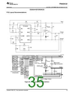
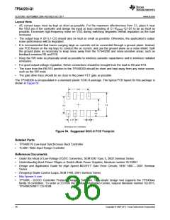
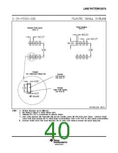
The TPS40200 is encapsulated in a standard plastic SOIC-8 package. The typical PCB layout for this package is
shown in Figure 54.
3.81
3
7.4
5.2
2.2
0.6
1.27
Dimensions are in millimeters
Figure 54. Suggested SOIC-8 PCB Footprint
Related Parts
•
•
TPS4007/9 Low-Input Synchronous Buck Controller
TL5001 Wide-Input-Range Controller
Reference Documents
•
•
•
Under the Hood of Low-Voltage DC/DC Converters, SEM1500 Topic 5, 2002 Seminar Series
Understanding Buck Power Stages in Switch-Mode Power Supplies, literature number SLVA057
Design and Application Guide for High Speed MOSFET Gate Drive Circuits, SEM 1400 – 2001 Seminar
Series
•
•
•
Designing Stable Control Loops, SEM 1400, 2001 Seminar Series
http://power.ti.com
TPS40K - DC/DC Controller Products Designer Software. This simple design tool supports the TPS40xxx
family of controllers. To order a CD from the Product Information Center, request literature number SLU015,
TPS40K/SWIFT CD-ROM.
36
Copyright © 2006–2011, Texas Instruments Incorporated

 TI [ TEXAS INSTRUMENTS ]