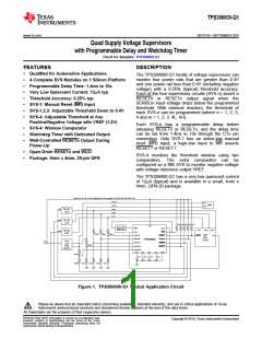
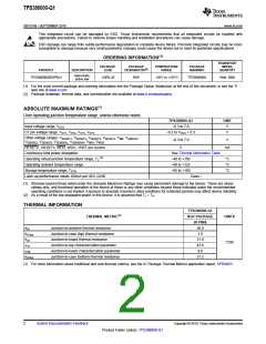
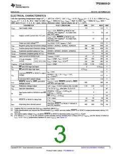
TPS386000-Q1
www.ti.com
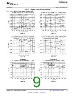
SBVS149 –SEPTEMBER 2010
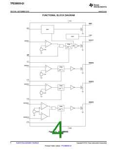
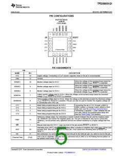
PIN CONFIGURATIONS
RGP PACKAGE
QFN-20
(TOP VIEW)
1
2
3
4
5
15
14
13
12
11
MR
CT4
CT3
CT2
CT1
RESET1
VCC
VREF
GND
(Thermal Pad)
NC
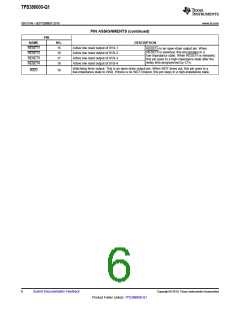
PIN ASSIGNMENTS
PIN
NAME
VCC
NO.
14
DESCRIPTION
Supply voltage. Connecting a 0.1mF ceramic capacitor close to this pin is recommended.
GND
12
Ground
When the voltage at this terminal drops below the
threshold voltage (VITN), RESET1 is asserted.
SENSE1
SENSE2
SENSE3
SENSE4L
10
9
Monitor voltage input to SVS-1
Monitor voltage input to SVS-2
Monitor voltage input to SVS-3
When the voltage at this terminal drops below the
threshold voltage (VITN), RESET2 is asserted.
When the voltage at this terminal drops below the
threshold voltage (VITN), RESET3 is asserted.
8
Falling monitor voltage input to SVS-4. When the voltage at this terminal drops below the threshold
voltage (VITN), RESET4 or RESET4 is asserted.
7
Rising monitor voltage input to SVS-4. When the voltage at this terminal exceeds the threshold voltage
(VITP), RESET4 or RESET4 is asserted. This pin can also be used to monitor the negative voltage rail
in combination with VREF pin.
SENSE4H
6
CT1
CT2
CT3
5
4
3
Reset delay programming pin for SVS-1
Reset delay programming pin for SVS-2
Reset delay programming pin for SVS-3
Connecting this pin to VCC through a 40kΩ to
200kΩ resistor, or leaving it open, selects a fixed
delay time (see the Electrical Characteristics).
Connecting a capacitor > 220pF between this pin
and GND selects the programmable delay time
(see the Reset Delay Time section).
CT4
2
Reset delay programming pin for SVS-4
Reference voltage output. By connecting a resistor network between this pin and the negative power
rail, SENSE4H can monitor the negative power rail. This pin is intended to only source current into
resistor(s). Do not connect only capacitors and do not connect resistor(s) to a higher voltage than this
pin.
VREF
13
MR
1
Manual reset input for SVS-1. Logic low level of this pin asserts RESET1 or RESET1.
Watchdog timer (WDT) trigger input. Inputting either a positive or negative logic edge every 610ms (typ)
prevents WDT time out at the WDO or WDO pin. Timer starts from releasing event of RESET1 or
RESET1.
WDI
20
NC
11
Not connected. It is recommended to connect this pin to the GND pin (pin 12), which is next to this pin.
This is the IC substrate. This pad must be connected only to GND or to the floating thermal pattern on
the printed circuit board (PCB).
(Thermal Pad)
(PAD)
Copyright © 2010, Texas Instruments Incorporated
Submit Documentation Feedback
5
Product Folder Link(s): TPS386000-Q1

 TI [ TEXAS INSTRUMENTS ]