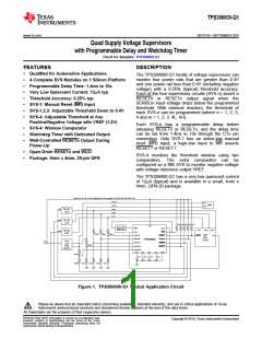
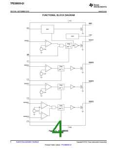
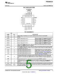
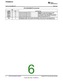
TPS386000-Q1
www.ti.com
SBVS149 –SEPTEMBER 2010
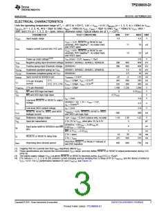
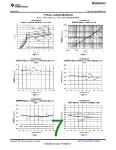
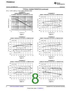
ELECTRICAL CHARACTERISTICS
Over the operating temperature range of TJ = –40°C to +125°C, 1.8V < VVCC < 6.5V, RRESETn (n = 1, 2, 3, 4) = 100kΩ to VVCC
,
CRESETn (n = 1, 2, 3, 4L, 4H) = 50pF to GND, RWDO = 100kΩ to VVCC, CWDO = 50pF to GND, VMR = 100kΩ to VVCC, WDI =
GND, and CTn (n = 1, 2, 3, 4) = open, unless otherwise noted. Typical values are at TJ = +25°C.
PARAMETER
TEST CONDITIONS
MIN
TYP
MAX UNIT
VVCC
Input supply range
1.8
6.5
V
VVCC = 3.3V, RESETn or RESETn not
asserted, WDI toggling(1), no output load,
and VREF open
11
13
19
mA
IVCC
Supply current (current into VCC pin)
Power-up reset voltage(2)(3)
VVCC = 6.5V, RESETn or RESETn not
asserted, WDI toggling(1), no output load,
and VREF open
22
mA
VOL (max) = 0.2V, IRESETn = 15mA
0.9
404
V
mV
mV
mV
mV
nA
nA
nA
V
VITN
Negative-going input threshold voltage SENSE1, SENSE2, SENSE3, SENSE4L
Positive-going input threshold voltage SENSE4H
396
396
400
400
3.5
VITP
404
VHYSN
VHYSP
ISENSE
Hysteresis (positive-going) on VITN
Hysteresis (negative-going) on VITP
Input current at SENSEm pin
SENSE1, SENSE2, SENSE3, SENSE4L
SENSE4H
10
3.5
10
VSENSEm = 0.42V
CCT1 > 220pF, VCT1 = 0.5V(4)
CT2, CT3, CT4 CCTn > 220pF, VCTn = 0.5V(4)
–25
245
±1
+25
CT1
300
300
1.238
355
CTn pin charging
ICT
current
235
365
VTH(CTn) CTn pin threshold
CCTn > 220pF
1.180
0
1.299
0.3VVCC
VIL
VIH
MR and WDI logic low input
V
MR and WDI logic high input
0.7VVCC
V
IOL = 1mA
0.4
0.3
V
Low-level RESETn or RESETn output
voltage
SENSEn = 0V, 1.3V < VVCC < 1.8V,
IOL = 0.4mA(2)
VOL
V
V
Low-level WDO output voltage
IOL = 1mA
0.4
RESETn, RESETn, WDO, and WDO
leakage current
VRESETn = 6.5V, RESETn, RESETn, WDO,
and WDO are logic high
ILKG
–300
1.18
300
1.22
nA
VREF
CIN
Reference voltage output
Input pin capacitance
1mA < IVREF < 0.2mA (source only, no sink)
1.20
5
V
CTn: 0V to VVCC, other pins: 0V to 6.5V
pF
SENSEm: 1.05VITN → 0.95VITN or
0.95VITP → 1.05VITP
4
ms
Input pulse width to SENSEm and MR
pins
tW
MR: 0.7VCC → 0.3VVCC
CTn = open
1
20
ns
ms
ms
14
24
tD
RESETn or RESETn delay time
Watchdog timer timeout period
CTn = VVCC
225
300
375
Start from RESET1 or RESET1 release or
last WDI transition
tWDT
450
600
750
ms
(1) Toggling WDI for a period less than tWDT negatively affects IVCC
.
(2) These specifications are beyond the recommended VVCC range, and only define RESETn or RESETn output performance during VCC
ramp up.
(3) The lowest supply voltage (VVCC) at which RESETn or RESETn becomes active; tRISE(VCC) ≥ 15ms/V.
(4) CTn (where n = 1, 2, 3, or 4) are constant current charging sources working from a range of 0V to VTH(CTn), and the device is tested at
VCTn = 0.5V. For ICT performance between 0V and VTH(CTn), see Figure 23.
Copyright © 2010, Texas Instruments Incorporated
Submit Documentation Feedback
3
Product Folder Link(s): TPS386000-Q1

 TI [ TEXAS INSTRUMENTS ]