TPS20xxC
SLVSAU6A –JUNE 2011–REVISED JULY 2011
www.ti.com
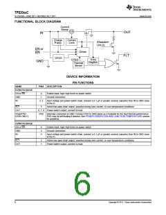
FUNCTIONAL BLOCK DIAGRAM
Current
Sense
CS
OUT
IN
Charge
Pump
Current
Limit
(Disabled+
UVLO)
EN or
EN
Driver
FLT
UVLO
9-ms
Deglitch
OTSD
Thermal
Sense
GND
DEVICE INFORMATION
PIN FUNCTIONS
NAME
PINS DESCRIPTION
8-PIN PACKAGE
EN or EN
GND
4
1
Enable input, logic high turns on power switch
Ground connection
IN
2, 3
Input voltage and power-switch drain; connect a 0.1 µF or greater ceramic capacitor from IN to GND close
to the IC
FLT
5
Active-low open-drain output, asserted during over-current, or over-temperature conditions
OUT
6, 7, 8 Power-switch output, connect to load
PowerPAD
(DGN ONLY)
PAD
Internally connected to GND. Connect PAD to GND plane as a heatsink for the best thermal performance.
PAD may be left floating if desired. See POWER DISSIPATION AND JUNCTION TEMPERATURE section
for guidance.
5-PIN PACKAGE
EN or EN
GND
4
2
5
Enable input, logic high turns on power switch
Ground connection
IN
Input voltage and power-switch drain; connect a 0.1 µF or greater ceramic capacitor from IN to GND close
to the IC
FLT
3
1
Active-low open-drain output, asserted during over-current, or over-temperature conditions
Power-switch output, connect to load.
OUT
6
Copyright © 2011, Texas Instruments Incorporated

 TI [ TEXAS INSTRUMENTS ]