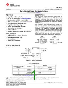
TPS20xxC
SLVSAU6A –JUNE 2011–REVISED JULY 2011
www.ti.com
This integrated circuit can be damaged by ESD. Texas Instruments recommends that all integrated circuits be handled with
appropriate precautions. Failure to observe proper handling and installation procedures can cause damage.
ESD damage can range from subtle performance degradation to complete device failure. Precision integrated circuits may be more
susceptible to damage because very small parametric changes could cause the device not to meet its published specifications.
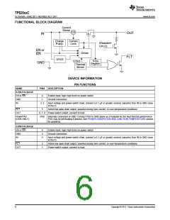
DEVICE INFORMATION(1)
PACKAGED DEVICE(2)
MAXIMUM
OPERATING
CURRENT
OUTPUT
DISCHARGE
BASE PART
NUMBER
ENABLE
MARKING
MSOP-8 (DGN)
PowerPAD™
SOT23-5
(DBV)
0.5
1
Y
Y
Y
Y
Y
High
High
High
Low
High
TPS2051C
TPS2065C
TPS2069C
TPS2000C
TPS2001C
–
√
√
√
√
√
√
–
–
–
VBYQ
VCAQ
VBUQ
BCMS
VBWQ
1.5
2
2
(1) For the most current packaging and ordering information, see the Package Option Addendum at the end of this document, or see the TI
website at www.ti.com.
(2) "-" indicates the device is not available in this package.
ABSOLUTE MAXIMUM RATINGS(1)(2)
VALUE
UNIT
MIN
–0.3
–6
MAX
(3)
Voltage range on IN, OUT, EN or EN, FLT
Voltage range from IN to OUT
Maximum junction temperature, TJ
HBM
6
6
V
V
Internally Limited
2
kV
V
Electrostatic Discharge
CDM
IEC 61000-4-2, Contact / Air
500
(4)
8
15
kV
(1) Absolute maximum ratings apply over recommended junction temperature range.
(2) Voltages are with respect to GND unless otherwise noted.
(3) See the Input and Output Capacitance section.
(4) VOUT was surged on a pcb with input and output bypassing per Figure 1 (except input capacitor was 22 µF) with no device failures.
THERMAL INFORMATION
0.5 A or 1 A 1.5 A or 2 A 0.5 A or 1 A 1.5 A or 2 A
THERMAL METRIC(1)
(See DEVICE INFORMATION table.)
Rated
DBV
5 PINS
224.9
95.2
Rated
DBV
5 PINS
220.4
89.7
Rated
DGN
8 PINS
72.1
Rated
DGN
8 PINS
67.1
UNITS
θJA
Junction-to-ambient thermal resistance
Junction-to-case (top) thermal resistance
Junction-to-board thermal resistance
θJCtop
θJB
87.3
80.8
51.4
46.9
42.2
37.2
ψJT
Junction-to-top characterization parameter
Junction-to-board characterization parameter
Junction-to-case (bottom) thermal resistance
6.6
5.2
7.3
5.6
°C/W
ψJB
50.3
46.2
42.0
36.9
θJCbot
N/A
N/A
39.2
32.1
See the Power DIssipation and Junction
Temperature section
θJACustom
139.3
134.9
66.5
61.3
(1) For more information about traditional and new thermal metrics, see the IC Package Thermal Metrics application report, SPRA953.
2
Copyright © 2011, Texas Instruments Incorporated

 TI [ TEXAS INSTRUMENTS ]