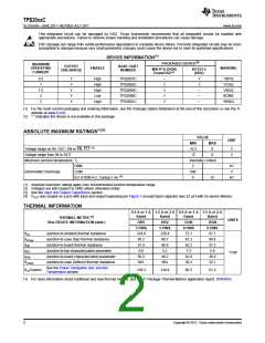
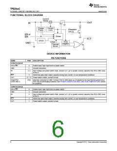
TPS20xxC
SLVSAU6A –JUNE 2011–REVISED JULY 2011
www.ti.com
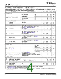
ELECTRICAL CHARACTERISTICS: –40°C ≤ TJ ≤ 125°C
Unless otherwise noted:4.5 V ≤ VIN ≤ 5.5 V, VEN = VIN or VEN = GND, IOUT = 0 A, typical values are at 5 V and 25°C. See the
DEVICE INFORMATION table for the rated current of each part number.
PARAMETER
POWER SWITCH
TEST CONDITIONS(1)
MIN
TYP
MAX
UNIT
0.5 A rated output
1 A rated output
DBV
97
96
86
69
72
154
154
140
112
112
mΩ
mΩ
DBV
DGN
DGN
DGN
RDS(ON) Input – output resistance
1.5 A rated output
2 A rated output
mΩ
mΩ
ENABLE INPUT (EN or EN)
Threshold
Input rising
1
0.07
–1
1.45
0.13
0
2
0.20
1
V
V
Hysteresis
Leakage current
(VEN or VEN) = 0 V or 5.5 V
µA
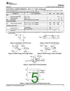
VIN = 5 V, CL = 1 µF, RL = 100 Ω, EN ↑ or EN ↓.
See Figure 2, Figure 4, and Figure 5
tON
Turnon time
Turnoff time
ms
ms
0.5A / 1A Rated
1.5A / 2A Rated
1
1.4
1.7
1.8
2.2
1.2
VIN = 5 V, CL = 1 µF, RL = 100 Ω, EN ↓ or EN ↑.
See Figure 2, Figure 4, and Figure 5
tOFF
0.5A and 1A Rated
1.3
1.7
1.65
2.1
2
1.5A / 2A Rated
2.5
CL = 1 µF, RL = 100 Ω, VIN = 5 V. See Figure 3
0.5A / 1A Rated
tR
Rise time, output
Fall time, output
0.4
0.5
0.55
0.7
0.7
1.0
ms
ms
1.5A / 2A Rated
CL = 1 µF, RL = 100 Ω, VIN = 5 V. See Figure 3
0.5A / 1A Rated
tF
0.25
0.3
0.35
0.43
0.45
0.55
1.5A / 2A Rated
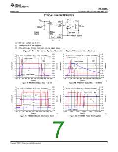
CURRENT LIMIT
0.5 A rated
output
0.65
1.2
1.6
2.3
0.85
1.55
2.15
2.9
1.05
1.9
2.7
3.6
1 A rated output
Current-limit,
See Figure 8
(2)
IOS
A
1.5 A rated
output
2 A rated output
VIN = 5 V (see Figure 7),
One-half full load → RSHORT = 50 mΩ,
Measure from application to when current falls below
120% of final value
tIOS
Short-circuit response time(3)
2
µs
SUPPLY CURRENT
ISD
Supply current, switch disabled
0.01
65
10
90
20
µA
µA
µA
ISE
Supply current, switch enabled
Reverse leakage current
IREV
VOUT = 5.5 V, VIN = 0 V, Measure IVOUT
0.2
UNDERVOLTAGE LOCKOUT
VUVLO
Rising threshold
Hysteresis(3)
VIN
↑
↓
3.5
3.75
0.14
4
V
V
VIN
(1) Pulsed testing techniques maintain junction temperature approximately equal to ambient temperature
(2) See CURRENT LIMIT section for explanation of this parameter.
(3) These parameters are provided for reference only, and do not constitute part of TI's published device specifications for purposes of TI's
product warranty.
4
Copyright © 2011, Texas Instruments Incorporated

 TI [ TEXAS INSTRUMENTS ]