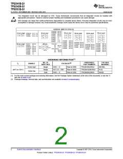
TPS2041B-Q1
TPS2042B-Q1
TPS2051B-Q1
SLVS782A –NOVEMBER 2007–REVISED JUNE 2010
www.ti.com
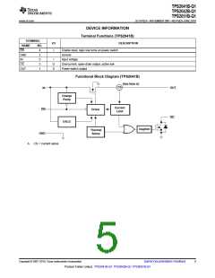
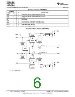
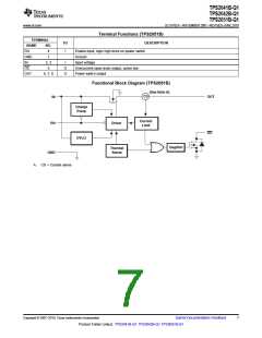
Terminal Functions (TPS2042B)
TERMINAL
I/O
DESCRIPTION
NAME
EN1
NO.
3
I
I
Enable input, logic low turns on power switch IN-OUT1
Enable input, logic low turns on power switch IN-OUT2
Ground
EN2
GND
IN
4
1
2
I
Input voltage
OC1
OC2
OUT1
OUT2
8
O
O
O
O
Overcurrent, open-drain output, active low, IN-OUT1
Overcurrent, open-drain output, active low, IN-OUT2
Power-switch output, IN-OUT1
5
7
6
Power-switch output, IN-OUT2
Functional Block Diagram (TPS2042B)
OC1
Thermal
Deglitch
Sense
GND
EN1
Current
Driver
Limit
Charge
Pump
(See Note A)
CS
OUT1
OUT2
UVLO
(See Note A)
IN
CS
Charge
Pump
Current
Driver
Limit
OC2
EN2
Thermal
Sense
Deglitch
A. CS = Current sense
6
Submit Documentation Feedback
Copyright © 2007–2010, Texas Instruments Incorporated
Product Folder Link(s): TPS2041B-Q1 TPS2042B-Q1 TPS2051B-Q1

 TI [ TEXAS INSTRUMENTS ]