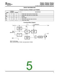
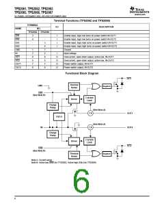
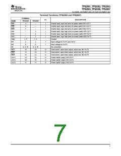
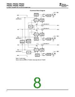
TPS2061, TPS2062, TPS2063
TPS2065, TPS2066, TPS2067
www.ti.com
SLVS490B–DECEMBER 2003–REVISED DECEMBER 2004
ABSOLUTE MAXIMUM RATINGS
over operating free-air temperature range unless otherwise noted(1)
UNIT
-0.3 V to 6 V
-0.3 V to 6 V
-0.3 V to 6 V
-0.3 V to 6 V
Internally limited
See Dissipation Rating Table
-40°C to 125°C
-65°C to 150°C
260°C
(2)
Input voltage range, VI(IN)
Output voltage range, VO(OUT)(2), VO(OUTx)
Input voltage range, VI(/EN), VI(EN), VI(/ENx), VI(ENx)
Voltage range, VI(/OC), VI(/OCx)
Continuous output current, IO(OUT), IO(OUTx)
Continuous total power dissipation
Operating virtual junction temperature range, TJ
Storage temperature range, Tstg
Lead temperature soldering 1,6 mm (1/16 inch) from case for 10 seconds
Human body model MIL-STD-883C
Electrostatic discharge (ESD) protection
2 kV
Charge device model (CDM)
500 V
(1) Stresses beyond those listed under absolute maximum ratings may cause permanent damage to the device. These are stress ratings
only, and functional operation of the device at these or any other conditions beyond those indicated under recommended operating
conditions is not implied. Exposure to absolute-maximum-rated conditions for extended periods may affect device reliability.
(2) All voltages are with respect to GND.
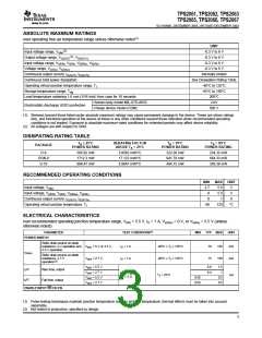
DISSIPATING RATING TABLE
T
A ≤ 25°C
DERATING FACTOR
ABOVE TA = 25°C
TA = 70°C
POWER RATING
TA = 85°C
POWER RATING
PACKAGE
POWER RATING
D-8
DGN-8
D-16
585.82 mW
5.8582 mW/°C
17.123 mW/°C
8.9847 mW/°C
322.20 mW
941.78 mW
494.15 mW
234.32 mW
684.33 mW
359.38 mW
1712.3 mW
898.47 mW
RECOMMENDED OPERATING CONDITIONS
MIN
MAX UNIT
Input voltage, VI(IN)
2.7
0
5.5
5.5
1
V
V
Input voltage, VI(/EN), VI(EN), VI(/ENx), VI(ENx)
Continuous output current, IO(OUT), IO(OUTx)
Operating virtual junction temperature, TJ
0
A
-40
125
°C
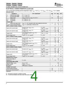
ELECTRICAL CHARACTERISTICS
over recommended operating junction temperature range, VI(IN) = 5.5 V, IO = 1 A, VI(/ENx) = 0 V, or VI(ENx) = 5.5 V (unless
otherwise noted)
PARAMETER
POWER SWITCH
TEST CONDITIONS(1)
MIN
TYP MAX
UNIT
Static drain-source on-state
resistance, 5-V operation and VI(IN) = 5 V or 3.3 V,
3.3-V operation
IO = 1 A
IO = 1 A
-40°C ≤ TJ ≤ 125°C
-40°C ≤ TJ ≤ 125°C
70
75
135
150
mΩ
mΩ
rDS(on)
Static drain-source on-state
resistance, 2.7-V
operation(2)
VI(IN) = 2.7 V,
VI(IN) = 5.5 V
VI(IN) = 2.7 V
VI(IN) = 5.5 V
VI(IN) = 2.7 V
0.6
0.4
1.5
1
(2)
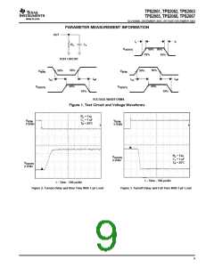
tr
Rise time, output
Fall time, output
CL = 1 µF,
RL = 5 Ω
TJ = 25°C
ms
0.05
0.05
0.5
0.5
tf(2)
ENABLE INPUT EN OR EN
(1) Pulse-testing techniques maintain junction temperature close to ambient temperature; thermal effects must be taken into account
separately.
(2) Not tested in production, specified by design.
3

 TI [ TEXAS INSTRUMENTS ]