TPS2061, TPS2062, TPS2063
TPS2065, TPS2066, TPS2067
www.ti.com
SLVS490B–DECEMBER 2003–REVISED DECEMBER 2004
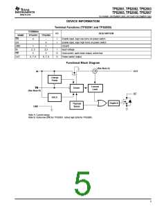
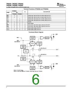
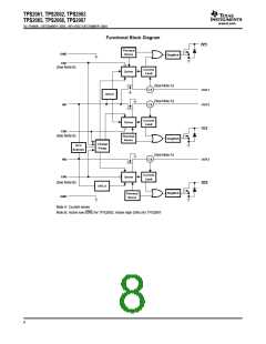
Functional Block Diagram
OC1
Thermal
Sense
GND
Deglitch
EN1
(See Note B)
Current
Driver
Limit
(See Note A)
CS
CS
OUT1
OUT2
UVLO
(See Note A)
IN1
Current
Limit
Driver
OC2
EN2
(See Note B)
Thermal
Sense
Deglitch
Charge
Pump
VCC
Selector
(See Note A)
IN2
CS
OUT3
OC3
Current
Limit
EN3
Driver
(See Note B)
UVLO
Deglitch
Thermal
Sense
GND
Note A: Current sense
Note B: Active low (ENx) for TPS2063; Active high (ENx) for TPS2067
8

 TI [ TEXAS INSTRUMENTS ]