TPS1HC30-Q1
ZHCSP75A –JULY 2022 –REVISED DECEMBER 2022
www.ti.com.cn
9.4 Layout
9.4.1 Layout Guidelines
To prevent thermal shutdown, TJ must be less than 150°C. If the output current is very high, the power
dissipation can be large. The HTSSOP package has good thermal impedance. However, the PCB layout is very
important. Good PCB design can optimize heat transfer, which is absolutely essential for the long-term reliability
of the device.
• Maximize the copper coverage on the PCB to increase the thermal conductivity of the board. The major heat-
flow path from the package to the ambient is through the copper on the PCB. Maximum copper is extremely
important when there are not any heat sinks attached to the PCB on the other side of the board opposite the
package.
• Add as many thermal vias as possible directly under the package ground pad to optimize the thermal
conductivity of the board.
• Plate shut or plug and cap all thermal vias on both sides of the board to prevent solder voids. To ensure
reliability and performance, the solder coverage must be at least 85%.
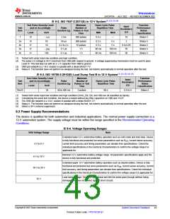
9.4.2 Layout Example
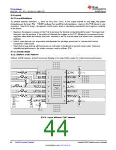
9.4.2.1 Without a GND Network
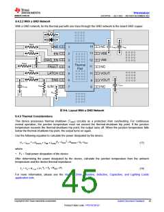
Without a GND network, tie the thermal pad directly to the board GND copper for better thermal performance.
RPROT
14
CVBB
GND
NC
1
2
3
4
5
6
7
RPROT
13
VBB
VBB
EN
DIAG_EN
FAULT
12
11
RPU
RPROT
Thermal
Pad
NC
RPROT
10
LATCH
SNS
VOUT
VOUT
NC
RPROT
9
8
RSNS
CFILTER
CVOUT
ILIM
RLIM
图9-5. Layout Without a GND Network
Copyright © 2023 Texas Instruments Incorporated
44
Submit Document Feedback
Product Folder Links: TPS1HC30-Q1

 TI [ TEXAS INSTRUMENTS ]