TPS1HC100-Q1
ZHCSLK6A –JULY 2021 –REVISED DECEMBER 2021
www.ti.com.cn
(2) Device will function within extended operating range, however some timing parametric values might not apply. See the respective
sections for what voltages are used. Additionally more explanation can be found in Power Supply Recommendations
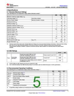
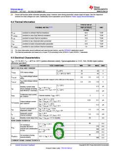
6.4 Thermal Information
TPS1HC100-Q1
THERMAL METRIC(1) (2)
PWP (HTSSOP)
UNIT
14 PINS
42.6
34.7
13.8
0.7
RθJA
Junction-to-ambient thermal resistance
Junction-to-case (top) thermal resistance
Junction-to-board thermal resistance
°C/W
°C/W
°C/W
°C/W
°C/W
°C/W
RθJC(top)
RθJB
Junction-to-top characterization parameter
Junction-to-board characterization parameter
Junction-to-case (bottom) thermal resistance
ψJT
14.0
1.8
ψJB
RθJC(bot)
(1) For more information about traditional and new thermal metrics, see the SPRA953 application report.
(2) The thermal parameters are based on a 4-layer PCB according to the JESD51-5 and JESD51-7 standards.
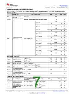
6.5 Electrical Characteristics
VBB = 6 V to 28 V, TA = -40°C to 125°C (unless otherwise noted); Typical application is 13.5V, 10Ω, RILIM=Open (unless
otherwise specified)
PARAMETER
TEST CONDITIONS
MIN
TYP
MAX
UNIT
INPUT VOLTAGE AND CURRENT
TJ=25°C
35
33
43
45
V
V
VClamp
VDS clamp voltage
TJ = -40°C to 150°C
VBB undervoltage lockout
rising
VUVLOR
VUVLOF
3.0
2.4
3.5
2.6
4.0
3.0
0.3
0.5
V
V
Measured with respect to the GND pin of the device
VBB undervoltage lockout
falling
TJ = 25°C
µA
µA
A
Standby current (total
device leakage including
both MOSFET channels)
VBB ≤28 V, VEN
=
ISB
VDIA_EN = 0 V, VOUT = 0 V
TJ = 85°C
Continuous load current,
per channel
INOM
Channel enabled, TAMB = 85°C
2
VBB ≤28 V, TJ = 25°C
VEN = VDIA_EN = 0 V, VOUT = 0 V
0.01
0.1
0.3
1.5
2.5
µA
µA
mA
Output leakage current
(per channel)
IOUT(standby)
VBB ≤28 V, TJ = 85°C
VEN = VDIA_EN = 0 V, VOUT = 0 V
Current consumption in
diagnostic mode
VBB ≤28 V, ISNS = 0 mA
VEN = 0 V, VDIA_EN = 5 V, VOUT = 0V
IDIA
1.3
Quiescent current
channel enabled
VBB ≤28 V
VEN = VDIA_EN = 5 V, IOUTx = 0 A
IQ
1.6
20
mA
ms
tSTBY
Standby mode delay time VENx = VDIA_EN = 0 V to standby
RON CHARACTERISTICS
TJ = 25°C
TJ = 150°C
TJ = 25°C
TJ = 150°C
TJ = 25°C
TJ = 150°C
88
mΩ
mΩ
mΩ
mΩ
mΩ
mΩ
6 V ≤VBB ≤28 V,
IOUT= 1 A
On-resistance
(Includes MOSFET
channel and metallization
on die)
176
190
250
RON
3V ≤VBB ≤6V,
IOUT =1A
94
On-resistance during
reverse polarity
RON(REV)
-18 V ≤VBB ≤-6 V
188
CURRENT SENSE CHARACTERISTICS
Copyright © 2022 Texas Instruments Incorporated
6
Submit Document Feedback
Product Folder Links: TPS1HC100-Q1

 TI [ TEXAS INSTRUMENTS ]