TPS1HC100-Q1
ZHCSLK6A –JULY 2021 –REVISED DECEMBER 2021
www.ti.com.cn
8 Detailed Description
8.1 Overview
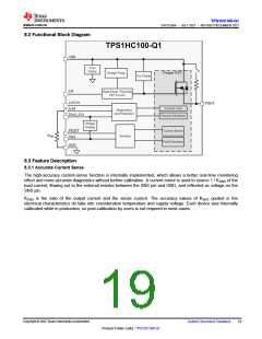
The TPS1HC100-Q1 is a single-channel, fully-protected, high-side power switch with an integrated NMOS power
FET and charge pump. Full diagnostics and high-accuracy current-sense features enable intelligent control of
the load. Low logic high threshold, VIH, of 1.5 V on the input pins allow use of MCU GPIO signals of 1.8 V. A
programmable current-limit function greatly improves the reliability of the whole system. The device diagnostic
reporting has two pins to support both digital status and analog current-sense output, both of which can be set to
the high-impedance state when diagnostics are disabled, for multiplexing the MCU analog or digital interface
among devices.
The digital status report is implemented with an open-drain structure on the fault pin. When a fault condition
occurs, the pin is pulled down to GND. An external pullup is required to match the microcontroller supply level.
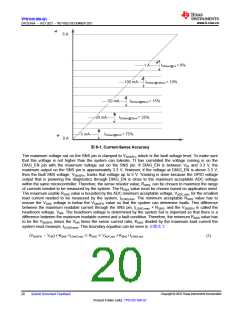
High-accuracy current sensing allows a better real-time monitoring effect and more-accurate diagnostics without
further calibration. A current mirror is used to source 1 / KSNS of the load current, which is reflected as voltage on
the SNS pin. KSNS is a constant value across the temperature and supply voltage. The current-sensing function
operates normally within a wide linear region from 0 to 4 V. The SNS pin can also report a fault by forcing a
voltage of VSNSFH that scales with the diagnostic enable voltage so that the maximum voltage seen by the
system's ADC is within an acceptable value. This action removes the need for an external zener diode or resistor
divider on the SNS pin.
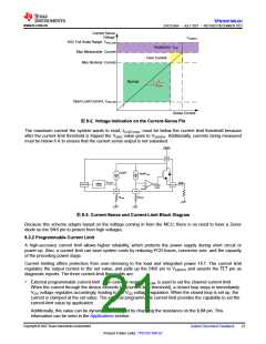
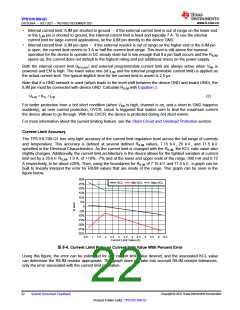
The external high-accuracy current limit allows setting the current limit value by application. The current limit
highly improves the reliability of the system by clamping the inrush current effectively under start-up or short-
circuit conditions. Also, the current limit can save system costs by reducing PCB trace, connector size, and the
preceding power-stage capacity. An internal current limit is also implemented in this device. The lower value of
the external or internal current-limit value is applied.
An active drain to source voltage clamp is built in to address switching off the energy of inductive loads, such as
relays, solenoids, pumps, motors, and so forth. During the inductive switching-off cycle, both the energy of the
power supply (EBAT) and the load (ELOAD) are dissipated on the high-side power switch itself. With the benefits of
process technology and excellent IC layout, the TPS1HC100-Q1 device can achieve excellent power dissipation
capacity, which can help save the external free-wheeling circuitry in most cases. For more details, see Inductive-
Load Switching-Off Clamp.
Short-circuit reliability is critical for smart high-side power-switch devices. The standard of AEC-Q100-012 is to
determine the reliability of the devices when operating in a continuous short-circuit condition. Different grade
levels are specified according to the pass cycles. This device is qualified with the highest level, Grade A, 1
million times short-to-GND certification.
The TPS1HC100-Q1 device can be used as a high-side power switch for a wide variety of resistive, inductive,
and capacitive loads, including the low-wattage bulbs, LEDs, relays, solenoids, and heaters.
Copyright © 2022 Texas Instruments Incorporated
18
Submit Document Feedback
Product Folder Links: TPS1HC100-Q1

 TI [ TEXAS INSTRUMENTS ]