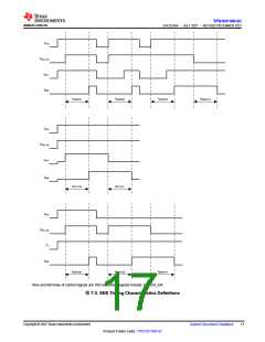
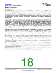
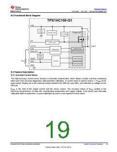
TPS1HC100-Q1
ZHCSLK6A –JULY 2021 –REVISED DECEMBER 2021
www.ti.com.cn
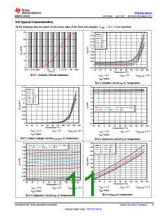
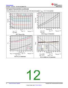
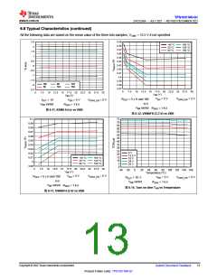
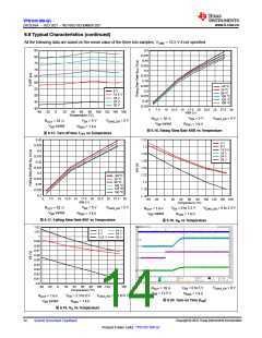
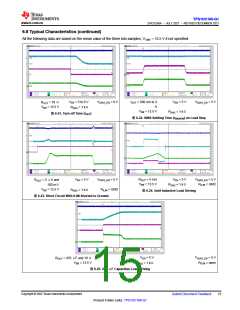
6.8 Typical Characteristics (continued)
All the following data are based on the mean value of the three lots samples, VVBB = 13.5 V if not specified.
VEN = 5 to 0 V
VDIAG_EN = 0 V
IOUT = 500 mA to 3
VEN = 5 V
VDIAG_EN = 5 V
ROUT = 10 Ω
A
VBB = 13.5 V
RSNS = 1 kΩ
VBB = 13.5 V
RSNS = 1 kΩ
图6-21. Turn-off Time (tOFF
)
图6-22. ISNS Settling Time (tSNSION) on Load Step
VEN = 5 V
VDIAG_EN = 5 V
RILIM = GND
ROUT = 5 mH
VBB = 13.5 V
VEN = 5 V
VDIAG_EN = 5 V
RILIM = GND
ROUT = 5 μH and
100 mΩ
RSNS = 1 kΩ
VBB = 13.5 V
RSNS = 1 kΩ
图6-24. 5mH Inductive Load Driving
图6-23. Short Circuit With ILIM Shorted to Ground
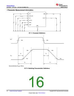
VEN = 5 V
VDIAG_EN = 5 V
RILIM = open
ROUT = 470 μF and 10 Ω
VBB = 13.5 V
RSNS = 1 kΩ
图6-25. 470-μF Capacitive Load Driving
Copyright © 2022 Texas Instruments Incorporated
Submit Document Feedback
15
Product Folder Links: TPS1HC100-Q1

 TI [ TEXAS INSTRUMENTS ]