TPS1H100-Q1
ZHCSDD8D –OCTOBER 2014–REVISED DECEMBER 2019
www.ti.com.cn
Feature Description (continued)
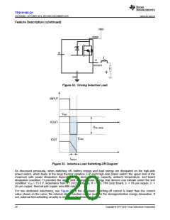
VBAT
DRAIN
IN
L
-
-
SOURCE
+
GND
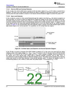
Figure 32. Driving Inductive Load
INPUT
VBAT
VOUT
IOUT
VDS, clamp
EHSD
tDECAY
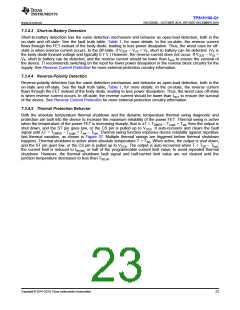
Figure 33. Inductive-Load Switching-Off Diagram
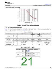
As discussed previously, when switching off, battery energy and load energy are dissipated on the high-side
power switch, which leads to the large thermal variation. For each high-side power switch, the upper limit of the
maximum safe power dissipation depends on the device intrinsic capacity, ambient temperature, and board
dissipation condition. TI provides the upper limit of single-pulse energy that devices can tolerate under the test
condition: VVS = 13.5 V, inductance from 0.1 mH to 400 mH, R = 0 Ω, FR4 2s2p board, 2- × 70-μm copper, 2- ×
35-μm copper, thermal pad copper area 600 mm2.
For one dedicated inductance, see Figure 34. If the maximum switching-off current is lower than the current
value shown on the curve, the internal clamp function can be used for the demagnetization energy dissipation. If
not, external free-wheeling circuitry is necessary for device protection.
20
Copyright © 2014–2019, Texas Instruments Incorporated

 TI [ TEXAS INSTRUMENTS ]