TPS1H100-Q1
www.ti.com.cn
ZHCSDD8D –OCTOBER 2014–REVISED DECEMBER 2019
Feature Description (continued)
•
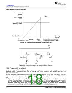
Internal current limit -- The internal current limit is fixed and typically 10 A. To use the internal current limit for
large-current applications, tie the CL pin directly to the device GND.
Both the internal current limit (Ilim,nom) and external programmable current limit are always active when VVS is
powered and IN is high. The lower one (of Ilim,nom and the external programmable current limit) is applied as the
actual current limit.
Note that if a GND network is used (which leads to the level shift between the device GND and board GND), the
CL pin must be connected with device GND. Calculate RCL with Equation 2.
VCL,th
VCL,th ì KCL
Iout
ICL
=
=
ç RCL =
RCL
KCL
Iout
(2)
For better protection from a hard short-to-GND condition (when VS and input are high and a short to GND
happens suddenly), an open-loop fast-response behavior is set to turn off the channel, before the current-limit
closed loop is set up. The open-loop response time is around 1 µs. With this fast response, the device can
achieve better inrush-suppression performance.
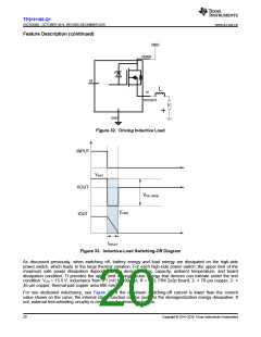
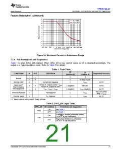
7.3.3 Inductive-Load Switching-Off Clamp
When an inductive load is switching off, the output voltage is pulled down to negative, due to the inductance
characteristics. The power FET may break down if the voltage is not clamped during the current-decay period. To
protect the power FET in this situation, internally clamp the drain-to-source voltage, namely VDS,clamp, the clamp
diode between the drain and gate.
VDS,clamp = VBAT œ VOUT
(3)
During the current-decay period (TDECAY), the power FET is turned on for inductance-energy dissipation. Both the
energy of the power supply (EBAT) and the load (ELOAD) are dissipated on the high-side power switch itself, which
is called EHSD. If resistance is in series with inductance, some of the load energy is dissipated in the resistance.
EHSD = EBAT + ELOAD = EBAT +EL œ ER
(4)
From the high-side power switch’s view, EHSD equals the integration value during the current-decay period.
TDECAY
EHSD
=
VDS,clamp ì IOUT(t)dt
—
0
(5)
(6)
(7)
≈
’
R ì IOUT(MAX) + VOUT
L
∆
∆
«
÷
÷
◊
TDECAY
=
ì ln
R
VOUT
»
ÿ
Ÿ
VBAT + VOUT
≈ R ì IOUT(MAX) + VOUT
’
…
ì R ì IOUT(MAX) œ VOUT ln
EHSD = L ì
∆
÷
÷
◊
R2
∆
VOUT
…
Ÿ
⁄
«
When R approximately equals 0, EHSD can be given simply as:
VBAT + VOUT
1
EHSD
=
ì L ì I2
OUT(MAX)
R2
(8)
2
Copyright © 2014–2019, Texas Instruments Incorporated
19

 TI [ TEXAS INSTRUMENTS ]