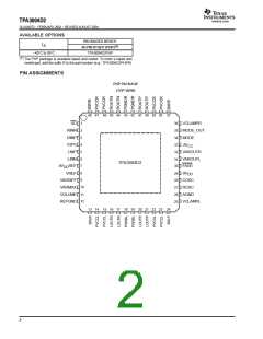
ꢀ
ꢁꢂ
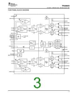
ꢃ
ꢄ
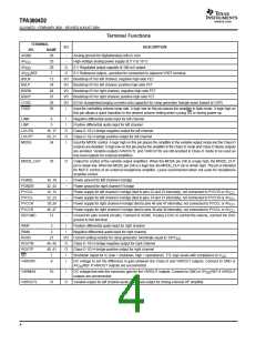
ꢄ
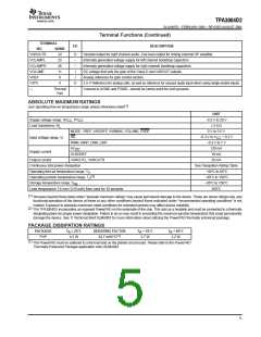
ꢅ
ꢆꢇ
www.ti.com
SLOS407D − FEBRUARY 2003 − REVISED AUGUST 2004
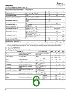
RECOMMENDED OPERATING CONDITIONS
MIN
8.5
MAX
UNIT
Supply voltage, V
18
V
PV , AV
CC
R ≥ 3.6 Ω
L
CC
CC;
Volume reference voltage
Volume control pins, input voltage
VREF
3.0
5.5
5.5
V
V
VARDIFF, VARMAX, VOLUME
SD
2
3.5
4.0
MODE
FADE
High-level input voltage, V
IH
V
SD
0.8
2
Low-level input voltage, V
IL
V
MODE, FADE
High-level output voltage, V
MODE_OUT, I
MODE_OUT, I
= 1 mA
AV −100 mV
DD
V
V
OH
OH
Low-level output voltage, V
= −1 mA
AGND+100 mV
OL
OL
MODE,V = 5 V, V
= 18 V
= 18 V
CC
1
150
50
I
CC
FADE, V = 5 V, V
High-level input current, I
uA
I
IH
SD, V = 18 V, V
CC
= 18 V
I
MODE, FADE , V = 0 V, V
CC
= 18 V
1
uA
uA
kHz
°C
I
Low-level input current, I
IL
SD, V = 0 V, V
CC
= 18 V
1
I
Oscillator frequency, f
OSC
225
−40
275
85
Operating free-air temperature, T
A
(1)
Operating junction temperature, T
125
°C
J
(1)
Continuous operation above the recommended junction temperature may result in reduced reliability and/or lifetime of the device. The junction
temperature is controlled by the thermal design of the application and should be carefully considered in high power dissipation applications. See
the thermal considerations section on pages 33−35 for recommendations on improving the thermal performance of your application.
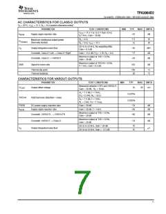
DC CHARACTERISTICS
T
A
= 25°C, V
CC
= 12 V, R = 8 Ω (unless otherwise noted)
L
PARAMETER
TEST CONDITIONS
MIN
TYP
10
MAX
UNIT
Class-D Output offset voltage
(measured differentially)
INN and INP connected together,
Gain = 36 dB
| V
OS
|
65
mV
0.45x
0.5x 0.55x
V2P5 (terminal 4)
2.5-V Bias voltage
No load
V
AV
AV
AV
DD
DD
DD
I
V
= 0 to 100 mA, SD = 2 V,
O
AV
DD
5-V Regulated output
4.5
5.0
5.5
V
= 8.5 V to 18 V
CC
PSRR
Class-D power supply rejection ratio
Class-D mode quiescent current
V
= 11.5 V to 12.5 V
−80
16
dB
mA
CC
MODE = 2 V, SD = 2 V,
= 18 V
I
I
I
28.5
9
CC(class-D)
V
CC
MODE = 3.5 V, SD = 2 V,
= 18 V
Variable output mode quiescent
current
7
mA
A
CC(varout)
V
CC
Class-D mode RMS current at max
power
R
= 8 Ω, P = 12 W,
L
O
2
1
CC(class-D – max power)
V
CC
= 15 V to 18 V
SD = 0.8 V, V
= 12 V
10
CC
CC
I
Supply current in shutdown mode
Drain-source on-state resistance
uA
CC(SD)
SD = 0.8 V, V
= 18 V
160
High side
Low side
Total
300
250
550
V
I
= 12 V,
CC
= 1 A,
r
mΩ
O
ds(on)
T = 25°C
J
650
6

 TI [ TEXAS INSTRUMENTS ]