www.ti.com
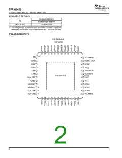
TERMINAL
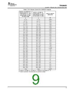
ꢀ ꢁꢂ ꢃꢄꢄ ꢅꢆ ꢇ
SLOS407D − FEBRUARY 2003 − REVISED AUGUST 2004
Terminal Functions (Continued)
I/O
DESCRIPTION
NO.
VAROUTR
VCLAMPL
VCLAMPR
VOLUME
VREF
NAME
32
25
36
11
8
O
−
−
I
Variable output for right channel audio. Line level output for driving external HP amplifier.
Internally generated voltage supply for left channel bootstrap capacitors.
Internally generated voltage supply for right channel bootstrap capacitors.
DC voltage that sets the gain of the Class-D and VAROUT outputs.
I
Analog reference for gain control section.
V2P5
4
O
−
2.5-V Reference for analog cells, as well as reference for unused audio input when using single-ended inputs.
Connect to AGND and PGND—should be center point for both grounds.
—
Thermal
Pad
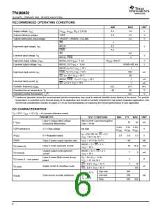
ABSOLUTE MAXIMUM RATINGS
over operating free-air temperature range unless otherwise noted
(1)
UNIT
−0.3 V to 20 V
≥ 3.6 Ω
Supply voltage range: AV
CC,
PV
CC
Load impedance, R
L
MODE, VREF, VARDIFF, VARMAX, VOLUME, FADE
0 V to 5.5 V
SD
−0.3 V to V
+ 0.3 V
Input voltage range, V
CC
I
RINN, RINP, LINN, LINP
−0.3 V to 7 V
AV
DD
120 mA
10 mA
Supply current
Output current
AVDDREF
VAROUTL, VAROUTR
20 mA
Continuous total power dissipation
Operating free-air temperature range, T
See Dissipation Rating Table
−40°C to 85°C
−40°C to 150°C
−65°C to 150°C
260°C
A
(2)
Operating junction temperature range, T
J
Storage temperature range, T
stg
Lead temperature 1,6 mm (1/16 inch) from case for 10 seconds
(1)
(2)
Stresses beyond those listed under “absolute maximum ratings” may cause permanent damage to the device. These are stress ratings only, and
functional operation of the device at these or any other conditions beyond those indicated under “recommended operating conditions” is not
implied. Exposure to absolute-maximum-rated conditions for extended periods may affect device reliability.
The TPA3004D2 incorporates an exposed PowerPAD on the underside of the chip. This acts as a heatsink and must be connected to a thermally
dissipating plane for proper power dissipation. Failure to do so may result in exceeding the maximum junction temperature that could permanently
damage the device. See TI Technical Brief SLMA002 for more information about utilizing the PowerPAD thermally enhanced package.
PACKAGE DISSIPATION RATINGS
PACKAGE
T
A
≤ 25°C
DERATING FACTOR
T
A
= 70°C
T = 85°C
A
(1)
PHP
4.3 W
34.7 mW/°C
2.7 W
2.2 W
(1)
The PowerPAD must be soldered to a thermal land on the printed circuit board. Please refer to the PowerPAD
Thermally Enhanced Package application note (SLMA002
5

 TI [ TEXAS INSTRUMENTS ]