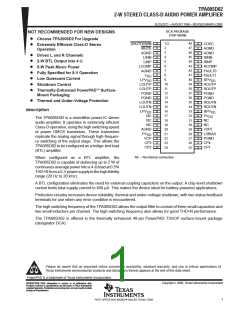
TPA005D02
2-W STEREO CLASS-D AUDIO POWER AMPLIFIER
SLOS227C – AUGUST 1998 – REVISED MARCH 2000
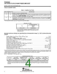
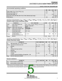
recommended operating conditions
MIN NOM
4.5
MAX
UNIT
Supply voltage, PV , LPV , RPV , V
DD DD
5.5
V
V
V
DD
DD
High-level input voltage, V
4.25
IH
Low-level input voltage, V
0.75
1
IL
Audio inputs, LINN, LINP, RINN, RINP, HPLIN, HPRIN, differential input voltage
PWM frequency
V
RMS
kHZ
100
500
electrical characteristics, V
(resistive load) (unless otherwise noted)
= PV
= LPV
= RPV
= 5 V, R = 4 Ω, T = 25°C, See Figure 1
DD
DD
DD
DD
L
C
PARAMETER
TEST CONDITIONS
= LPV = RPV = 4.9 V to 5.1 V
MIN
TYP
40
MAX
UNIT
dB
PSRR
Power supply rejection ratio
Supply current
V
= PV
DD DD
DD
DD
I
I
I
I
I
No load or output filter
MUTE = 0 V
25
40
15
mA
mA
µA
DD
Supply current, mute mode
Supply current, shutdown mode
High-level input current
Low-level input current
10
DD(MUTE)
SHUTDOWN = 0 V
400
2000
10
DD(SD)
V
= 5.3 V
µA
IH
IL
IH
IL
V
= –0.3 V
–10
µA
Total static drain-to-source
on-state resistance
(low-side plus high-side FETs)
r
r
I
D
= 0.5 A
620
750
mΩ
DS(on)
DS(on)
Matching
95%
99.5%
operating characteristics, V
(unless otherwise noted)
= PV
= LPV
= RPV
= 5 V, R = 4 Ω, T = 25°C, See Figure 1
DD
DD
DD
DD
L
C
PARAMETER
RMS output power, THD = 0.5%, per channel
TEST CONDITIONS
MIN
TYP
2
MAX
UNIT
P
O
W
THD+N Total harmonic distortion plus noise
Efficiency
P
= 1 W, f = 1 kHz
0.2%
80%
24
O
R
= 8 Ω
L
A
Gain
dB
V
Left/right channel gain matching
Noise floor
95%
60
dB
dB
Dynamic range
Crosstalk
70
f = 1 kHz
55
dB
Frequency response bandwidth, post output filter, –3 dB
Maximum output power bandwidth
20
20,000
20
Hz
B
OM
kHz
thermal resistance
PARAMETER
TEST CONDITIONS
MIN
TYP
MAX
UNIT
R
R
Thermal resistance, junction-to-pad
Thermal resistance, junction-to-pad
10
°C/W
θJP
θJA
†
22.3
°C/W
†
Please see the Texas Instruments document, PowerPAD Thermally Enhanced Package Application Report (literature number SLMA002), for
more information on the PowerPAD package. The thermal data was measured on a PCB layout based on the information in the section entitled
Texas Instruments Recommended Board for PowerPAD on page 33 of the before mentioned document.
5
POST OFFICE BOX 655303 • DALLAS, TEXAS 75265

 TI [ TEXAS INSTRUMENTS ]