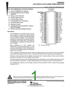
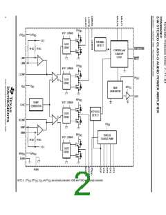
TPA005D02
2-W STEREO CLASS-D AUDIO POWER AMPLIFIER
SLOS227C – AUGUST 1998 – REVISED MARCH 2000
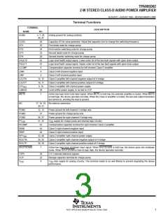
Terminal Functions
TERMINAL
NAME
AGND
DESCRIPTION
NO.
3, 7, 20,
46, 47
Analog ground for analog sections
COSC
CP1
48
25
Capacitor I/O for ramp generator. Adjust the capacitor size to change the switching frequency.
First diode node for charge pump
CP2
24
First inverter switching node for charge pump
CP3
23
Second diode node for charge pump
CP4
26
Second inverter switching node for charge pump
FAULT0
FAULT1
LCOMP
LINN
42
Logic level fault0 output signal. Lower order bit of the two fault signals with open drain output.
Logic level fault1 output signal. Higher order bit of the two fault signals with open drain output.
Compensation capacitor terminal for left-channel Class-D amplifier
Class-D left-channel negative input
41
6
4
LINP
5
Class-D left-channel positive input
LOUTN
LOUTP
14, 15
10, 11
9, 16
28
Class-D amplifier left-channel negative output of H-bridge
Class-D amplifier left-channel positive output of H-bridge
Class-D amplifier left-channel power supply
LPV
DD
LSBIAS
Level-shifter power supply, to be tied to VCP
2
MUTE
Active-low logic-level mute input signal. When MUTE is held low, the selected amplifier is muted. When MUTE
is held high, the device operates normally. When the Class-D amplifier is muted, the low-side output transistors
are turned on, shorting the load to ground.
NC
17, 18, 19, No internal connection
30, 31
PGND
PGND
PGND
12, 13
27
Power ground for left-channel H–bridge only
Power ground for charge pump only
36, 37
21, 32
43
Power ground for right-channel H-bridge only
PV
DD
V
DD
supply for charge-pump and internal logic circuitry
RCOMP
RINN
Compensation capacitor terminal for right-channel Class-D amplifier
Class-D right-channel negative input
45
RINP
44
Class-D right-channel positive input
RPV
DD
33, 40
34, 35
38, 39
1
Class-D amplifier right-channel power supply
ROUTN
Class-D amplifier right-channel negative output of H-bridge
Class-D amplifier right-channel positive output of H-bridge
ROUTP
SHUTDOWN
Active-low logic-level shutdown input signal. When SHUTDOWN is held low, the device goes into shutdown
mode. When SHUTDOWN is held at logic high, the device operates normally.
V2P5
VCP
29
22
8
2.5-V internal reference bypass
Storage capacitor terminal for charge pump
V
DD
V
bias supply for analog circuitry. This terminal needs to be well filtered to prevent degrading the device
DD
performance.
3
POST OFFICE BOX 655303 • DALLAS, TEXAS 75265

 TI [ TEXAS INSTRUMENTS ]