TMS570LS3137
www.ti.com
SPNS162.–SEPTEMBER 2011
3.3 Switching Characteristics over Recommended Operating Conditions for Clock Domains
Table 3-1. Clock Domain Timing Specifications
Parameter
fHCLK
Description
Conditions
Pipeline mode
Min
Max
Unit
HCLK - System clock frequency
PGE
160
MHz
enabled
Pipeline mode
disabled
45
180
45
MHz
MHz
MHz
ZWT
Pipeline mode
enabled
Pipeline mode
disabled
fGCLK
fVCLK
GCLK - CPU clock frequency
fHCLK
100
MHz
MHz
VCLK - Primary peripheral clock
frequency
fVCLK2
VCLK2 - Secondary peripheral clock
frequency
100
100
100
100
50
MHz
MHz
MHz
MHz
MHz
MHz
fVCLK3
VCLK3 - Secondary peripheral clock
frequency
fVCLKA1
fVCLKA2
fVCLKA4
fRTICLK
VCLKA1 - Primary asynchronous
peripheral clock frequency
VCLKA2 - Secondary asynchronous
peripheral clock frequency
VCLKA4 - Secondary asynchronous
peripheral clock frequency
RTICLK - clock frequency
fVCLK
3.4 Wait States Required
RAM
0
0
Address Waitstates
0MHz
fHCLK(max)
Data Waitstates
0MHz
fHCLK(max)
Flash
1
Address Waitstates
0
120MHz
fHCLK(max)
0MHz
Data Waitstates
0
1
2
3
fHCLK(max)
0MHz
45MHz
90MHz
135MHz
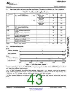
Figure 3-1. ZWT Wait States Scheme
As shown in the figure above, the TCM RAM can support program and data fetches at full CPU speed without
any address or data wait states required.
The TCM flash can support zero address and data wait states up to a CPU speed of 45MHz in non-pipelined
mode. The flash supports a maximum CPU clock speed of 160MHz in pipelined mode for the PGE Package and
180MHz for the ZWT package, with one address wait state and three data wait states.
The flash wrapper defaults to non-pipelined mode with zero address wait state and one random-read data wait
state.
Copyright © 2011, Texas Instruments Incorporated
Device Operating Conditions
43
Submit Documentation Feedback
focus.ti.com: TMS570LS3137

 TI [ TEXAS INSTRUMENTS ]