ꢀ ꢁ ꢂ ꢃ ꢄꢅ ꢆ ꢇ ꢄꢈꢈ ꢉ ꢀꢁ ꢂꢃ ꢄ ꢅ ꢆꢇ ꢄ ꢈꢈ ꢊ
ꢋ ꢌ ꢍꢎꢏ ꢐꢑ ꢒꢌ ꢓ ꢀ ꢏ ꢌ ꢔꢌ ꢀꢕꢖ ꢂ ꢌ ꢔꢓ ꢕꢖ ꢑ ꢗꢒ ꢆꢎꢂ ꢂꢒ ꢗꢂ
SPRS073L − AUGUST 1998 − REVISED JUNE 2005
Table of Contents
revision history . . . . . . . . . . . . . . . . . . . . . . . . . . . . . . . . . . . . . . 3
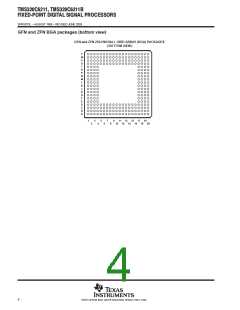
GFN and ZFN BGA packages (bottom view) . . . . . . . . . . . . 4
description . . . . . . . . . . . . . . . . . . . . . . . . . . . . . . . . . . . . . . . . . 5
device characteristics . . . . . . . . . . . . . . . . . . . . . . . . . . . . . . . . 6
device compatibility . . . . . . . . . . . . . . . . . . . . . . . . . . . . . . . . . . 7
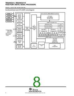
functional block and CPU (DSP core) diagram . . . . . . . . . . . 8
CPU (DSP core) description . . . . . . . . . . . . . . . . . . . . . . . . . . 9
memory map summary . . . . . . . . . . . . . . . . . . . . . . . . . . . . . . 11
peripheral register descriptions . . . . . . . . . . . . . . . . . . . . . . . 12
PWRD bits in CPU CSR register description . . . . . . . . . . . 17
EDMA channel synchronization events . . . . . . . . . . . . . . . . 18
interrupt sources and interrupt selector . . . . . . . . . . . . . . . . 19
signal groups description . . . . . . . . . . . . . . . . . . . . . . . . . . . . 20
terminal functions . . . . . . . . . . . . . . . . . . . . . . . . . . . . . . . . . . 22
development support . . . . . . . . . . . . . . . . . . . . . . . . . . . . . . . . 30
documentation support . . . . . . . . . . . . . . . . . . . . . . . . . . . . . . 33
clock PLL . . . . . . . . . . . . . . . . . . . . . . . . . . . . . . . . . . . . . . . . . 34
power-down logic . . . . . . . . . . . . . . . . . . . . . . . . . . . . . . . . . . . 36
power-supply sequencing . . . . . . . . . . . . . . . . . . . . . . . . . . . . 39
IEEE 1149.1 JTAG compatibility statement . . . . . . . . . . . . . 40
EMIF device speed . . . . . . . . . . . . . . . . . . . . . . . . . . . . . . . . . 40
bootmode . . . . . . . . . . . . . . . . . . . . . . . . . . . . . . . . . . . . . . . . . 41
absolute maximum ratings over operating case
temperature range . . . . . . . . . . . . . . . . . . . . . . . . . . 42
recommended operating conditions . . . . . . . . . . . . . . . . 42
electrical characteristics over recommended ranges of
supply voltage and operating case temperature . 42
parameter measurement information . . . . . . . . . . . . . . . 43
signal transition levels . . . . . . . . . . . . . . . . . . . . . . . . . . 43
timing parameters and board routing analysis . . . . . . 44
input and output clocks . . . . . . . . . . . . . . . . . . . . . . . . . . . 46
asynchronous memory timing . . . . . . . . . . . . . . . . . . . . . 49
synchronous-burst memory timing . . . . . . . . . . . . . . . . . 52
synchronous DRAM timing . . . . . . . . . . . . . . . . . . . . . . . . 54
HOLD/HOLDA timing . . . . . . . . . . . . . . . . . . . . . . . . . . . . 60
BUSREQ timing . . . . . . . . . . . . . . . . . . . . . . . . . . . . . . . . . 61
reset timing . . . . . . . . . . . . . . . . . . . . . . . . . . . . . . . . . . . . . 62
external interrupt timing . . . . . . . . . . . . . . . . . . . . . . . . . . 64
host-port interface timing . . . . . . . . . . . . . . . . . . . . . . . . . 65
multichannel buffered serial port timing . . . . . . . . . . . . . 69
timer timing . . . . . . . . . . . . . . . . . . . . . . . . . . . . . . . . . . . . . 80
JTAG test-port timing . . . . . . . . . . . . . . . . . . . . . . . . . . . . 81
mechanical data . . . . . . . . . . . . . . . . . . . . . . . . . . . . . . . . . 82
2
POST OFFICE BOX 1443 • HOUSTON, TEXAS 77251−1443

 TI [ TEXAS INSTRUMENTS ]