TMS320 SECOND-GENERATION
DEVICES
SPRS010B — MAY 1987 — REVISED NOVEMBER 1990
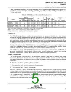
Table 1 provides an overview of the second-generation TMS320 processors with comparisons of memory, I/O,
cycle timing, power, package type, technology, and military support. For specific availability, contact the nearest
TI Field Sales Office.
Table 1. TMS320 Second-Generation Device Overview
MEMORY
PACKAGE
TYPE
CYCLE
TIME
(ns)
TYP
POWER
(mW)
†
I/O
ON-CHIP
OFF-CHIP
DEVICE
TIMER
RAM ROM/EPROM PROG DATA
SER
YES
YES
YES
YES
PAR
DMA
YES
CON
CON
CON
PGA PLCC CER-QUAD
‡
(NMOS)
(CMOS)
(CMOS)
(CMOS)
544
544
544
544
—
4K
4K
4K
64K
64K
64K
64K
64K
64K
64K
64K
YES
YES
YES
YES
200
100
80
1250
500
500
500
68
68
—
—
—
68
68
—
—
—
—
68
TMS32020
16 × 16
16 × 16
16 × 16
16 × 16
‡
TMS320C25
§
TMS320C25-50
§
TMS320E25
100
†
‡
§
SER = serial; PAR = parallel; DMA = direct memory access; CON = concurrent DMA.
Military version available; contact nearest TI Field Sales Office for availability.
Military version planned; contact nearest TI Field Sales Office for details.
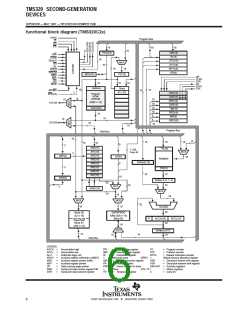
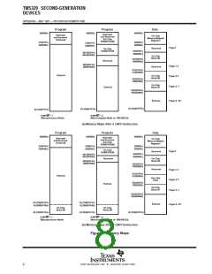
architecture
The TMS320 family utilizes a modified Harvard architecture for speed and flexibility. In a strict Harvard
architecture, program and data memory lie in two separate spaces, permitting a full overlap of instruction fetch
and execution. The TMS320 family’s modification of the Harvard architecture allows transfers between program
and data spaces, thereby increasing the flexibility of the device. This modification permits coefficients stored
in program memory to be read into the RAM, eliminating the need for a separate coefficient ROM. It also makes
available immediate instructions and subroutines based on computed values.
Increased throughput on the TMS320C2x devices for many DSP applications is accomplished by means of
single-cycle multiply/accumulate instructions with a data move option, up to eight auxiliary registers with a
dedicated arithmetic unit, and faster I/O necessary for data-intensive signal processing.
The architectural design of the TMS320C2x emphasizes overall speed, communication, and flexibility in
processor configuration. Control signals and instructions provide floating-point support, block-memory
transfers, communication to slower off-chip devices, and multiprocessing implementations.
32-bit ALU/accumulator
The 32-bit Arithmetic Logic Unit (ALU) and accumulator perform a wide range of arithmetic and logical
instructions, the majority of which execute in a single clock cycle. The ALU executes a variety of branch
instructions dependent on the status of the ALU or a single bit in a word. These instructions provide the following
capabilities:
•
•
•
Branch to an address specified by the accumulator
Normalize fixed-point numbers contained in the accumulator
Test a specified bit of a word in data memory
One input to the ALU is always provided from the accumulator, and the other input may be provided from the
Product Register (PR) of the multiplier or the input scaling shifter which has fetched data from the RAM on the
databus. AftertheALUhasperformedthearithmeticorlogicaloperations, theresultisstoredintheaccumulator.
The 32-bit accumulator is split into two 16-bit segments for storage in data memory. Additional shifters at the
output of the accumulator perform shifts while the data is being transferred to the data bus for storage. The
contents of the accumulator remain unchanged.
POST OFFICE BOX 1443 • HOUSTON, TEXAS 77001
5

 TI [ TEXAS INSTRUMENTS ]