TMS320 SECOND-GENERATION
DEVICES
SPRS010B — MAY 1987 — REVISED NOVEMBER 1990
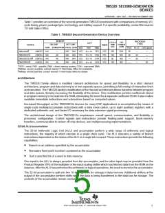
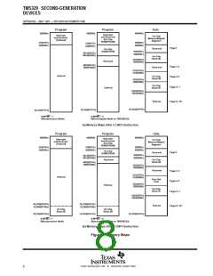
PGA AND PLCC/CER-QUAD PIN ASSIGNMENTS
FUNCTION
PIN
FUNCTION
A12
PIN
K8/40
L9/41
K9/42
L10/43
B7/68
G11/50
FUNCTION
D2
PIN
FUNCTION
D14
PIN
A5/3
FUNCTION
INT2
PIN
H1/22
J11/46
FUNCTION
PIN
A0
A1
A2
A3
A4
A5
A6
A7
A8
A9
A10
A11
K1/26
K2/28
L3/29
K3/30
L4/31
K4/32
L5/33
K5/34
K6/36
L7/37
K7/38
L8/39
E1/16
D2/15
D1/14
C2/13
C1/12
B2/11
A2/9
V
CC
V
CC
V
SS
V
SS
V
SS
H2/23
L6/35
A13
D3
D15
B6/2
IS
†
A14
D4
DR
J1/24
MP/MC A6/1
B1/10
K11/44
L2/27
A15
D5
DS
K10/45
E11/54
J2/25
MSC
PS
C10/59
J10/47
BIO
D6
DX
BR
D7
FSR
FSX
READY B8/66
XF
X1
D11/56
G10/51
CLKOUT1 C11/58
CLKOUT2 D10/57
D8
F10/53
A7/67
RS
A8/65
D9
B3/8
HOLD
R/W
H11/48
H10/49
F2/19
X2/CLKIN F11/52
CLKR
CLKX
D0
B9/64
A9/63
F1/18
E2/17
D10
D11
D12
D13
A3/7
HOLDA E10/55
STRB
SYNC
B4/6
IACK
INT0
INT1
B11/60
G1/20
G2/21
A4/5
V
V
A10/61
B10/62
CC
D1
B5/4
CC
†
On the TMS32020, MP/MC must be connected to V
CC
.
‡
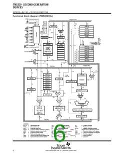
I/O/Z
SIGNALS
DEFINITION
V
V
I
I
5-V supply pins
Ground pins
CC
SS
X1
O
I
O
O
I/O/Z
O/Z
Output from internal oscillator for crystal
X2/CLKIN
CLKOUT1
CLKOUT2
D15-D0
A15-A0
PS, DS, IS
R/W
Input to internal oscillator from crystal or external clock
Master clock output (crystal or CLKIN frequency/4)
A second clock output signal
16-bit data bus D15 (MSB) through D0 (LSB). Multiplexed between program, data, and I/O spaces.
16-bit address bus A15 (MSB) through A0 (LSB)
O/Z
O/Z
Program, data, and I/O space select signals
Read/write signal
STRB
O/Z
Strobe signal
RS
I
I
I
O
O
I
Reset input
External user interrupt inputs
Microprocessor/microcomputer mode select pin
Microstate complete signal
Interrupt acknowledge signal
Data ready input. Asserted by external logic when using slower devices to indicate that the current bus transaction
INT2-INT0
MP/MC
MSC
IACK
READY
is complete.
BR
XF
HOLD
O
O
I
Bus request signal. Asserted when the TMS320C2x requires access to an external global data memory space.
External flag output (latched software-programmable signal)
Hold input. When asserted, TMS320C2x goes into an idle mode and places the data, address, and control lines in
the high impedance state.
HOLDA
SYNC
BIO
O
I
I
I
Hold acknowledge signal
Synchronization input
Branch control input. Polled by BIOZ instruction.
Serial data receive input
DR
CLKR
FSR
DX
CLKX
FSX
I
Clock for receive input for serial port
Frame synchronization pulse for receive input
Serial data transmit output
Clock for transmit output for serial port
I
O/Z
I
I/O/Z
Frame synchronization pulse for transmit. Configuration as either an input or an output.
‡
I/O/Z denotes input/output/high-impedance state.
POST OFFICE BOX 1443 • HOUSTON, TEXAS 77001
2

 TI [ TEXAS INSTRUMENTS ]