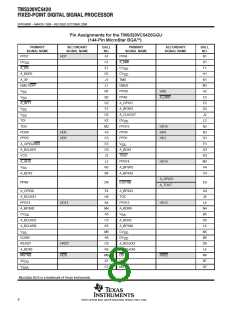
ꢀ ꢁ ꢂ ꢃ ꢄꢅ ꢆꢇ ꢈꢉꢄ ꢅ
ꢊ ꢋ ꢌꢍ ꢎꢏꢐ ꢑꢋ ꢒ ꢀ ꢎ ꢋ ꢓꢋ ꢀꢔꢕ ꢂ ꢋ ꢓꢒ ꢔꢕ ꢐ ꢖꢑ ꢇꢍꢂ ꢂꢑ ꢖ
SPRS080F − MARCH 1999 − REVISED OCTOBER 2008
Signal Descriptions (Continued)
†
NAME
TYPE
DESCRIPTION
MEMORY CONTROL SIGNALS (CONTINUED)
Data-ready input signal. READY indicates that the external device is prepared for a bus transaction to be
completed. If the device is not ready (READY = 0), the processor waits one cycle and checks READY again. The
processor performs the READY detection if at least two software wait states are programmed.
READY
I
This pin is also multiplexed with the HPI, and functions as the Host-port data ready (output) in HPI mode. Refer
to the HPI section of this table for details on the secondary function of this pin.
Read/write output signal. R/W indicates transfer direction during communication to an external device. R/W is
normally in the read mode (high), unless it is asserted low when the DSP performs a write operation.
This pin is also multiplexed with the HPI, and functions as the Host-port Read/write input in HPI mode. Refer to
the HPI section of this table for details on the secondary function of this pin.
R/W
O
O
This pin is placed into the high-impedance state when OFF is low.
I/O space memory strobe. External I/O space is accessible by the CPU and not the direct memory access (DMA)
controller. The DMA has its own dedicated I/O space that is not accessible by the CPU.
This pin is also multiplexed with the general pupose I/O feature, and functions as the A_GPIO3(A_TOUT) signal
in HPI mode. Refer to the general purpose I/O section of this table for details on the secondary function of this
pin.
IOSTRB
This pin is placed into the high-impedance state when OFF is low.
The SELA/B pin designates which DSP subsystem has access to the parallel-port interface. Furthermore, this
pin determines which subsystem is accessible by the host via the HPI.
For external memory accesses (XIO pin high), when SELA/B is low subsystem A has control of the external
memory interface. Similarly, when SELA/B is high subsystem B has control.
SELA/B
I
See Table 7 for a truth table of SELA/B, HMODE and XIO pins and functionality.
At device reset, the logic combination of the XIO, HMODE, and SELA/B pin levels determines the initialization
value of the MP/MC bit (a bit in the processor mode status (PMST) register ) Refer to the memory section for
details.
CLOCKING SIGNALS
Master clock output signal. CLKOUT cycles at the machine-cycle rate of the CPU. The internal machine cycle
is bounded by the falling edges of this signal. The CLKOUT pin can be turned off by writing a “1” to the CLKOFF
bit of the PMST register. CLKOUT goes into the high-impedance state when EMU1/OFF is low.
A_CLKOUT
B_CLKOUT
O
§
CLKIN
I
Input clock to the device. CLKIN connects to an oscillator circuit/device.
VCO is the output of the voltage-controlled oscillator stage of the PLL. This is a 3-state output during normal
operation. Active in silicon test/debug mode.
VCO
O
†
‡
§
¶
#
||
I = Input, O = Output, S = Supply, Z = High Impedance
This pin has an internal pullup resistor.
These pins have Schmitt trigger inputs.
This pin has an internal bus holder controlled by way of the BSCR register in subchip A.
This pin is used by Texas Instruments for device testing and should be left unconnected.
This pin has an internal pulldown resistor.
kAlthough this pin includes an internal pulldown resistor, a 470-Ω external pulldown is required. If the TRST pin is connected to multiple DSPs,
a buffer is recommended to ensure the V and V specifications are met.
IL
IH
12
POST OFFICE BOX 1443 • HOUSTON, TEXAS 77251−1443

 TI [ TEXAS INSTRUMENTS ]