ꢀ ꢁ ꢂ ꢃ ꢄꢅ ꢆꢇ ꢈꢉꢄ ꢅ
ꢊ ꢋ ꢌꢍ ꢎꢏꢐ ꢑꢋ ꢒ ꢀ ꢎ ꢋ ꢓꢋ ꢀꢔꢕ ꢂ ꢋ ꢓꢒ ꢔꢕ ꢐ ꢖꢑ ꢇꢍꢂ ꢂꢑ ꢖ
SPRS080F − MARCH 1999 − REVISED OCTOBER 2008
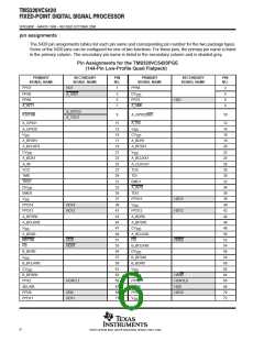
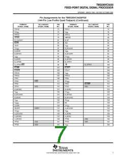
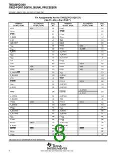
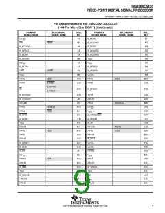
signal descriptions
The 5420 signal descriptions table lists each pin name, function, and operating mode(s) for the 5420 device.
Some of the 5420 pins can be configured for one of two functions; a primary function and a secondary function.
The names of these pins in secondary mode are shaded in grey in the following table.
Signal Descriptions
†
NAME
TYPE
DESCRIPTION
DATA SIGNALS
PPA17 (MSB)
PPA16
PPA15
PPA14
PPA13
PPA12
PPA11
PPA10
PPA9
Parallel port address bus. The DSP can access the external memory locations by way of the external memory
interface using PPA[17:0] in external memory interface (EMIF) mode when the XIO pin is logic high.
The PPA[17:0] pins are also multiplexed with the HPI interface. In HPI mode (XIO pin is low), the external address
pins PPA[17:0] are used by a host processor for access to the memory map by way of the on-chip HPI. Refer
to the HPI section of this table for details on the secondary functions of these pins.
I/O/Z
PPA8
PPA7
PPA6
PPA5
These pins are placed into the high-impedance state when OFF is low.
‡§
PPA4
PPA3
PPA2
PPA1
PPA0 (LSB)
PPD15 (MSB)
PPD14
PPD13
PPD12
PPD11
PPD10
PPD9
PPD8
PPD7
PPD6
PPD5
Parallel port data bus. The DSP uses this bidirectional data bus to access external memory when the device is
in external memory interface (EMIF) mode (the XIO pin is logic high).
This data bus is also multiplexed with the 16-bit HPI data bus. When in HPI mode, the bus is used to transfer data
between the host processor and internal DSP memory via the HPI. Refer to the HPI section of this table for details
on the secondary functions of these pins.
¶
I/O/Z
The data bus includes bus holders to reduce power dissipation caused by floating, unused pins. The bus holders
also eliminate the need for external pullup resistors on unused pins. When the data bus is not being driven by
the 5420, the bus holders keep data pins at the last driven logic level. The data bus keepers are disabled at reset
and can be enabled/disabled via the BH bit of the BSCR register.
PPD4
PPD3
PPD2
PPD1
These pins are placed into high-impedance state when OFF is low.
PPD0 (LSB)
INITIALIZATION, INTERRUPT, AND RESET OPERATIONS
§
§
§
§
A_INT0
B_INT0
A_INT1
B_INT1
External user interrupts. INT0−INT3 are prioritized and are maskable by the interrupt mask register (IMR) and
the interrupt mode bit. INT0 −INT3 can be polled and reset by way of the interrupt flag register (IFR).
I
I
§
§
A_NMI
B_NMI
Nonmaskable interrupt. NMI is an external interrupt that cannot be masked by way of the INTM or the IMR. When
NMI is activated, the processor traps to the appropriate vector location.
†
‡
§
¶
#
||
I = Input, O = Output, S = Supply, Z = High Impedance
This pin has an internal pullup resistor.
These pins have Schmitt trigger inputs.
This pin has an internal bus holder controlled by way of the BSCR register in subchip A.
This pin is used by Texas Instruments for device testing and should be left unconnected.
This pin has an internal pulldown resistor.
kAlthough this pin includes an internal pulldown resistor, a 470-Ω external pulldown is required. If the TRST pin is connected to multiple DSPs,
a buffer is recommended to ensure the V and V specifications are met.
IL
IH
10
POST OFFICE BOX 1443 • HOUSTON, TEXAS 77251−1443

 TI [ TEXAS INSTRUMENTS ]