TMS320F28027, TMS320F28027-Q1, TMS320F28027F, TMS320F28027F-Q1, TMS320F28026
TMS320F28026-Q1, TMS320F28026F, TMS320F28026F-Q1, TMS320F28023
TMS320F28023-Q1, TMS320F28022, TMS320F28021, TMS320F28020, TMS320F280200
ZHCSA13P –NOVEMBER 2008 –REVISED FEBRUARY 2021
www.ti.com.cn
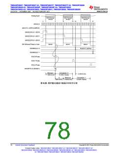
9.9.1.1.3 片载模数转换器(ADC) 电子数据/定时
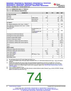
9.9.1.1.3.1 ADC Electrical Characteristics
PARAMETER
MIN
TYP
MAX
UNIT
DC SPECIFICATIONS
Resolution
12
0.001
7
Bits
ADC clock
60-MHz device
28027/26/23/22
28021/20/200
60
64
64
MHz
Sample Window
ADC
Clocks
14
ACCURACY
INL (Integral nonlinearity) at ADC Clock ≤30 MHz(1)
–4
–1
4
1
LSB
LSB
DNL (Differential nonlinearity) at ADC Clock ≤30 MHz,
no missing codes
Offset error (2)
Executing Device_Cal
function
0
0
20
4
–20
–4
LSB
Executing periodic self-
recalibration(3)
Overall gain error with internal reference
Overall gain error with external reference
Channel-to-channel offset variation
Channel-to-channel gain variation
ADC temperature coefficient with internal reference
ADC temperature coefficient with external reference
VREFLO
60
40
4
LSB
LSB
–60
–40
–4
LSB
4
LSB
–4
ppm/°C
ppm/°C
µA
–50
–20
–100
100
VREFHI
µA
ANALOG INPUT
Analog input voltage with internal reference
Analog input voltage with external reference
VREFLO input voltage(4)
0
VREFLO
VSSA
3.3
VREFHI
VSSA
V
V
V
VREFHI input voltage(5)
with VREFLO = VSSA
1.98
VDDA
V
Input capacitance
5
pF
μA
Input leakage current
±5
(1) INL will degrade when the ADC input voltage goes above VDDA
.
(2) 1 LSB has the weighted value of full-scale range (FSR)/4096. FSR is 3.3 V with internal reference and VREFHI - VREFLO for external
reference.
(3) Periodic self-recalibration will remove system-level and temperature dependencies on the ADC zero offset error. This can be
performed as needed in the application without sacrificing an ADC channel by using the procedure listed in the "ADC Zero Offset
Calibration" section of the Analog-to-Digital Converter and Comparator chapter in the TMS320F2802x,TMS320F2802xx Technical
Reference Manual.
(4) VREFLO is always connected to VSSA
.
(5) VREFHI must not exceed VDDA when using either internal or external reference modes. Because VREFHI is tied to ADCINA0 , the input
signal on ADCINA0 must not exceed VDDA
.
Copyright © 2022 Texas Instruments Incorporated
74
Submit Document Feedback
Product Folder Links: TMS320F28027 TMS320F28027-Q1 TMS320F28027F TMS320F28027F-Q1
TMS320F28026 TMS320F28026-Q1 TMS320F28026F TMS320F28026F-Q1 TMS320F28023 TMS320F28023-
Q1 TMS320F28022 TMS320F28021 TMS320F28020 TMS320F280200

 TI [ TEXAS INSTRUMENTS ]