TMS320F28027, TMS320F28027-Q1, TMS320F28027F, TMS320F28027F-Q1, TMS320F28026
TMS320F28026-Q1, TMS320F28026F, TMS320F28026F-Q1, TMS320F28023
TMS320F28023-Q1, TMS320F28022, TMS320F28021, TMS320F28020, TMS320F280200
ZHCSA13P –NOVEMBER 2008 –REVISED FEBRUARY 2021
www.ti.com.cn
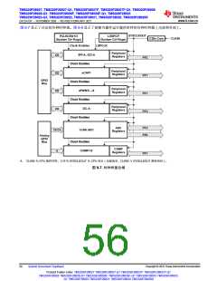
The PLL-based clock module provides four modes of operation:
• INTOSC1 (Internal Zero-pin Oscillator 1): This is the on-chip internal oscillator 1. This can provide the clock
for the Watchdog block, core and CPU-Timer 2
• INTOSC2 (Internal Zero-pin Oscillator 2): This is the on-chip internal oscillator 2. This can provide the clock
for the Watchdog block, core and CPU-Timer 2. Both INTOSC1 and INTOSC2 can be independently chosen
for the Watchdog block, core and CPU-Timer 2.
• Crystal/Resonator Operation: The on-chip (crystal) oscillator enables the use of an external crystal/
resonator attached to the device to provide the time base. The crystal/resonator is connected to the X1/X2
pins. Some devices may not have the X1/X2 pins. See 节7.2.1 for details.
• External Clock Source Operation: If the on-chip (crystal) oscillator is not used, this mode allows it to be
bypassed. The device clocks are generated from an external clock source input on the XCLKIN pin. The
XCLKIN is multiplexed with GPIO19 or GPIO38 pin. The XCLKIN input can be selected as GPIO19 or
GPIO38 through the XCLKINSEL bit in XCLK register. The CLKCTL[XCLKINOFF] bit disables this clock input
(forced low). If the clock source is not used or the respective pins are used as GPIOs, the user should disable
at boot time.
Before changing clock sources, ensure that the target clock is present. If a clock is not present, then that clock
source must be disabled (using the CLKCTL register) before switching clocks.
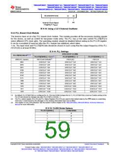
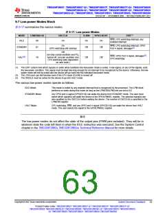
表9-16. Possible PLL Configuration Modes
CLKIN AND
SYSCLKOUT
PLL MODE
REMARKS
PLLSTS[DIVSEL]
Invoked by the user setting the PLLOFF bit in the PLLSTS register. The PLL block
is disabled in this mode. This can be useful to reduce system noise and for low-
power operation. The PLLCR register must first be set to 0x0000 (PLL Bypass)
before entering this mode. The CPU clock (CLKIN) is derived directly from the
input clock on either X1/X2, X1 or XCLKIN.
0, 1
2
3
OSCCLK/4
OSCCLK/2
OSCCLK/1
PLL Off
PLL Bypass is the default PLL configuration upon power-up or after an external
reset ( XRS). This mode is selected when the PLLCR register is set to 0x0000 or
while the PLL locks to a new frequency after the PLLCR register has been
modified. In this mode, the PLL is bypassed but the PLL is not turned off.
0, 1
2
3
OSCCLK/4
OSCCLK/2
OSCCLK/1
PLL Bypass
PLL Enable
0, 1
2
3
OSCCLK * n/4
OSCCLK * n/2
OSCCLK * n/1
Achieved by writing a nonzero value n into the PLLCR register. Upon writing to the
PLLCR the device will switch to PLL Bypass mode until the PLL locks.
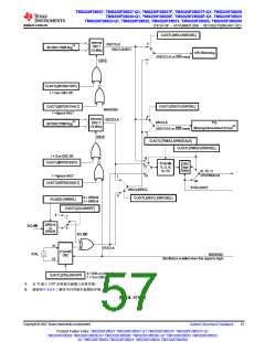
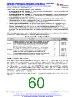
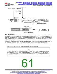
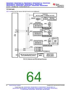
9.6.4 输入时钟的损耗(NMI 看门狗功能)
2802x 器件可由两个内部零引脚振荡器 (INTOSC1/INTOSC2) 的其中任一个、片上晶体振荡器、或者一个外部时
钟输入提供时钟信号。无论时钟源是什么,在 PLL 启用和 PLL 旁路模式中,如果到 PLL 的输入时钟消失,PLL
将在其输出上发出一个跛行模式时钟。这个跛行模式时钟持续为CPU 和外设提供一个典型值为1-5MHz 的时钟。
当跛行模式被激活时,一个被锁存为 NMI 中断的 CLOCLFAIL 信号被生成。根据 NMIRESETSEL 位的配置方
式,器件复位可能会被立即触发或者 NMI 看门狗计数器溢出时发出复位。除此之外,会设置丢失时钟状态
(MCLKSTS) 位。应用可使用 NMI 中断来检测输入时钟故障并启动所需的校正操作,例如切换到另一个时钟源
(如果有的话)或者为系统启动一个关断过程。
如果软件对于时钟故障情况没有响应,NMI 看门狗将在一个预编程的时间间隔后触发复位。图9-11 显示了涉及的
中断机制。
Copyright © 2022 Texas Instruments Incorporated
60
Submit Document Feedback
Product Folder Links: TMS320F28027 TMS320F28027-Q1 TMS320F28027F TMS320F28027F-Q1
TMS320F28026 TMS320F28026-Q1 TMS320F28026F TMS320F28026F-Q1 TMS320F28023 TMS320F28023-
Q1 TMS320F28022 TMS320F28021 TMS320F28020 TMS320F280200

 TI [ TEXAS INSTRUMENTS ]