TMS320F28027, TMS320F28027-Q1, TMS320F28027F, TMS320F28027F-Q1, TMS320F28026
TMS320F28026-Q1, TMS320F28026F, TMS320F28026F-Q1, TMS320F28023
TMS320F28023-Q1, TMS320F28022, TMS320F28021, TMS320F28020, TMS320F280200
ZHCSA13P –NOVEMBER 2008 –REVISED FEBRUARY 2021
www.ti.com.cn
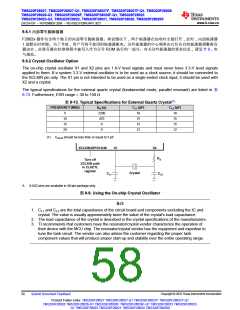
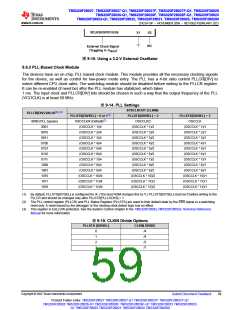
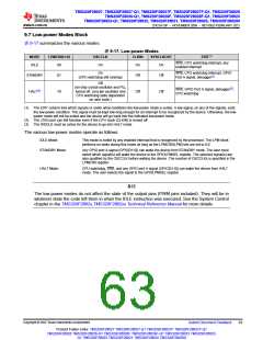
XCLKIN/GPIO19/38
X1
X2
NC
External Clock Signal
(Toggling 0−V
)
DDIO
图9-10. Using a 3.3-V External Oscillator
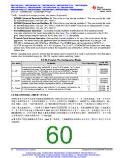
9.6.3 PLL-Based Clock Module
The devices have an on-chip, PLL-based clock module. This module provides all the necessary clocking signals
for the device, as well as control for low-power mode entry. The PLL has a 4-bit ratio control PLLCR[DIV] to
select different CPU clock rates. The watchdog module should be disabled before writing to the PLLCR register.
It can be re-enabled (if need be) after the PLL module has stabilized, which takes
1 ms. The input clock and PLLCR[DIV] bits should be chosen in such a way that the output frequency of the PLL
(VCOCLK) is at least 50 MHz.
表9-14. PLL Settings
SYSCLKOUT (CLKIN)
PLLCR[DIV] VALUE(2) (3)
PLLSTS[DIVSEL] = 0 or 1(1)
OSCCLK/4 (Default)(2)
(OSCCLK * 1)/4
PLLSTS[DIVSEL] = 2
OSCCLK/2
PLLSTS[DIVSEL] = 3
OSCCLK
0000 (PLL bypass)
0001
(OSCCLK * 1)/2
(OSCCLK * 2)/2
(OSCCLK * 3)/2
(OSCCLK * 4)/2
(OSCCLK * 5)/2
(OSCCLK * 6)/2
(OSCCLK * 7)/2
(OSCCLK * 8)/2
(OSCCLK * 9)/2
(OSCCLK * 10)/2
(OSCCLK * 11)/2
(OSCCLK * 12)/2
(OSCCLK * 1)/1
(OSCCLK * 2)/1
(OSCCLK * 3)/1
(OSCCLK * 4)/1
(OSCCLK * 5)/1
(OSCCLK * 6)/1
(OSCCLK * 7)/1
(OSCCLK * 8)/1
(OSCCLK * 9)/1
(OSCCLK * 10)/1
(OSCCLK * 11)/1
(OSCCLK * 12)/1
0010
(OSCCLK * 2)/4
0011
(OSCCLK * 3)/4
0100
(OSCCLK * 4)/4
0101
(OSCCLK * 5)/4
0110
(OSCCLK * 6)/4
0111
(OSCCLK * 7)/4
1000
(OSCCLK * 8)/4
1001
(OSCCLK * 9)/4
1010
(OSCCLK * 10)/4
(OSCCLK * 11)/4
(OSCCLK * 12)/4
1011
1100
(1) By default, PLLSTS[DIVSEL] is configured for /4. (The boot ROM changes this to /1.) PLLSTS[DIVSEL] must be 0 before writing to the
PLLCR and should be changed only after PLLSTS[PLLLOCKS] = 1.
(2) The PLL control register (PLLCR) and PLL Status Register (PLLSTS) are reset to their default state by the XRS signal or a watchdog
reset only. A reset issued by the debugger or the missing clock detect logic has no effect.
(3) This register is EALLOW protected. See the System Control chapter in the TMS320F2802x,TMS320F2802xx Technical Reference
Manual for more information.
表9-15. CLKIN Divide Options
PLLSTS [DIVSEL]
CLKIN DIVIDE
0
1
2
3
/4
/4
/2
/1
Copyright © 2022 Texas Instruments Incorporated
Submit Document Feedback
59
Product Folder Links: TMS320F28027 TMS320F28027-Q1 TMS320F28027F TMS320F28027F-Q1
TMS320F28026 TMS320F28026-Q1 TMS320F28026F TMS320F28026F-Q1 TMS320F28023 TMS320F28023-
Q1 TMS320F28022 TMS320F28021 TMS320F28020 TMS320F280200

 TI [ TEXAS INSTRUMENTS ]