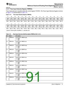
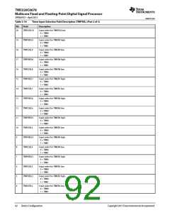
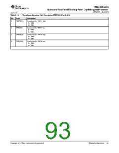
TMS320C6678
Multicore Fixed and Floating-Point Digital Signal Processor
SPRS691D—April 2013
www.ti.com
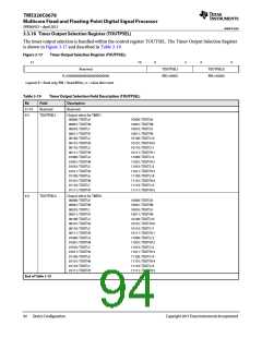
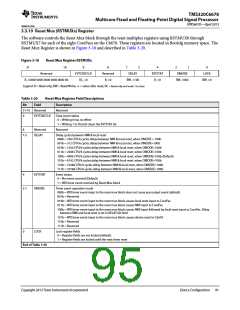
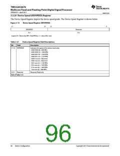
3.3.19 Reset Mux (RSTMUXx) Register
The software controls the Reset Mux block through the reset multiplex registers using RSTMUX0 through
RSTMUX7 for each of the eight CorePacs on the C6678. These registers are located in Bootcfg memory space. The
Reset Mux Register is shown in Figure 3-18 and described in Table 3-20.
Figure 3-18
Reset Mux Register RSTMUXx
31
10
9
8
7
5
4
3
1
0
Reserved
R, +0000 0000 0000 0000 0000 00
EVTSTATCLR
RC, +0
Reserved
R, +0
DELAY
RW, +100
EVTSTAT
R, +0
OMODE
RW, +000
LOCK
RW, +0
Legend: R = Read only; RW = Read/Write; -n = value after reset; RC = Read only and write 1 to clear
Table 3-20
Reset Mux Register Field Descriptions
Bit
Field
Description
31-10 Reserved
9
Reserved
EVTSTATCLR
Clear event status
0 = Writing 0 has no effect
1 = Writing 1 to this bit clears the EVTSTAT bit
8
Reserved
DELAY
Reserved
7-5
Delay cycles between NMI & local reset
000b = 256 CPU/6 cycles delay between NMI & local reset, when OMODE = 100b
001b = 512 CPU/6 cycles delay between NMI & local reset, when OMODE=100b
010b = 1024 CPU/6 cycles delay between NMI & local reset, when OMODE=100b
011b = 2048 CPU/6 cycles delay between NMI & local reset, when OMODE=100b
100b = 4096 CPU/6 cycles delay between NMI & local reset, when OMODE=100b (Default)
101b = 8192 CPU/6 cycles delay between NMI & local reset, when OMODE=100b
110b = 16384 CPU/6 cycles delay between NMI & local reset, when OMODE=100b
111b = 32768 CPU/6 cycles delay between NMI & local reset, when OMODE=100b
4
EVTSTAT
OMODE
Event status.
0 = No event received (Default)
1 = WD timer event received by Reset Mux block
3-1
Timer event operation mode
000b = WD timer event input to the reset mux block does not cause any output event (default)
001b = Reserved
010b = WD timer event input to the reset mux block causes local reset input to CorePac
011b = WD timer event input to the reset mux block causes NMI input to CorePac
100b = WD timer event input to the reset mux block causes NMI input followed by local reset input to CorePac. Delay
between NMI and local reset is set in DELAY bit field.
101b = WD timer event input to the reset mux block causes device reset to C6678
110b = Reserved
111b = Reserved
0
LOCK
Lock register fields
0 = Register fields are not locked (default)
1 = Register fields are locked until the next timer reset
End of Table 3-20
Copyright 2013 Texas Instruments Incorporated
Device Configuration 95

 TI [ TEXAS INSTRUMENTS ]