TMS320C6678
Multicore Fixed and Floating-Point Digital Signal Processor
SPRS691D—April 2013
www.ti.com
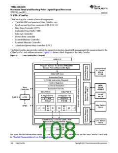
5.1 Memory Architecture
Each C66x CorePac of the TMS320C6678 device contains a 512KB level-2 memory (L2), a 32KB level-1 program
memory (L1P), and a 32KB level-1 data memory (L1D). The device also contain a 4096KB multicore shared memory
(MSM). All memory on the C6678 has a unique location in the memory map (see Table 2-2 ‘‘Memory Map
Summary’’ on page 21.
After device reset, L1P and L1D cache are configured as all cache, by default. The L1P and L1D cache can be
reconfigured via software through the L1PMODE field of the L1P Configuration Register (L1PCFG) and the
L1DMODE field of the L1D Configuration Register (L1DCFG) of the C66x CorePac. L1D is a two-way
set-associative cache, while L1P is a direct-mapped cache.
The on-chip bootloader changes the reset configuration for L1P and L1D. For more information, see the Bootloader
for the C66x DSP User Guide in ‘‘Related Documentation from Texas Instruments’’ on page 73.
For more information on the operation L1 and L2 caches, see the C66x DSP Cache User Guide in ‘‘Related
Documentation from Texas Instruments’’ on page 73.
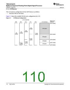
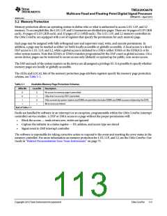
5.1.1 L1P Memory
The L1P memory configuration for the C6678 device is as follows:
•
32K bytes with no wait states
Figure 5-2 shows the available SRAM/cache configurations for L1P.
Figure 5-2
L1P Memory Configurations
L1P mode bits
010
Block base
address
00E0 0000h
000
001
011
100
L1P memory
16K bytes
1/2
SRAM
3/4
SRAM
7/8
SRAM
direct
mapped
cache
All
SRAM
00E0 4000h
00E0 6000h
8K bytes
direct
mapped
cache
4K bytes
4K bytes
direct
mapped
cache
00E0 7000h
00E0 8000h
dm
cache
Copyright 2013 Texas Instruments Incorporated
C66x CorePac 109

 TI [ TEXAS INSTRUMENTS ]