ꢀ ꢁ ꢂ ꢃ ꢄꢅ ꢆ ꢇ ꢈꢉ ꢈꢀꢊ ꢀꢁ ꢂꢃ ꢄ ꢅ ꢆꢇ ꢈ ꢉ ꢋꢀꢊ ꢀꢁ ꢂꢃ ꢄ ꢅ ꢆꢇ ꢈ ꢉ ꢇ ꢀ
ꢌ ꢍ ꢎꢏ ꢐꢑꢒ ꢓꢍ ꢔ ꢀ ꢐꢍ ꢕ ꢍ ꢀꢖꢗ ꢂ ꢍ ꢕꢔ ꢖꢗ ꢒ ꢘꢓ ꢆꢏ ꢂꢂꢓ ꢘꢂ
SPRS226H − NOVEMBER 2003 − REVISED AUGUST 2005
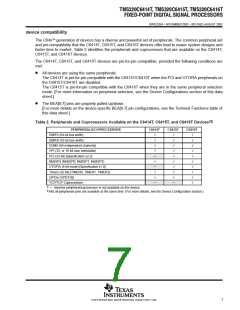
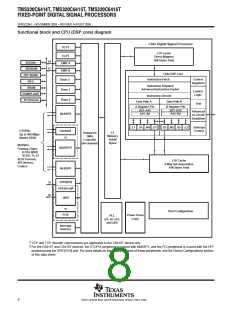
functional block and CPU (DSP core) diagram
C64x Digital Signal Processor
†
VCP
L1P Cache
Direct-Mapped
16K Bytes Total
†
TCP
64
16
SDRAM
EMIF A
EMIF B
SBSRAM
C64x DSP Core
ZBT SRAM
FIFO
Instruction Fetch
Control
Registers
Timer 2
Timer 1
Timer 0
Instruction Dispatch
Advanced Instruction Packet
SRAM
Control
Logic
ROM/FLASH
I/O Devices
Instruction Decode
Data Path A
Data Path B
Test
A Register File
A31−A16
B Register File
B31−B16
Advanced
In-Circuit
Emulation
McBSP2
A15−A0
B15−B0
.L1 .S1 .M1 .D1
.D2 .M2 .S2 .L2
Interrupt
Control
‡
UTOPIA:
UTOPIA
L2
Enhanced
DMA
Controller
(64-channel)
Up to 400 Mbps
Master ATMC
Memory
1024K
Bytes
or
McBSPs:
‡
McBSP1
McBSP0
Framing Chips:
H.100, MVIP,
SCSA, T1, E1
AC97 Devices,
SPI Devices,
Codecs
L1D Cache
2-Way Set-Associative
16K Bytes Total
GPIO[8:0]
16
32
‡
GPIO[15:9]
‡
HPI
or
Boot Configuration
‡
PCI
Power-Down
Logic
PLL
(x1, x6, x12,
and x20)
Interrupt
Selector
†
‡
VCP and TCP decoder coprocessors are applicable to the C6416T device only.
For the C6415T and C6416T devices, the UTOPIA peripheral is muxed with McBSP1, and the PCI peripheral is muxed with the HPI
peripheral and the GPIO[15:9] port. For more details on the multiplexed pins of these peripherals, see the Device Configurations section
of this data sheet.
8
POST OFFICE BOX 1443 • HOUSTON, TEXAS 77251−1443

 TI [ TEXAS INSTRUMENTS ]