TMDS361
www.ti.com ............................................................................................................................................................................................ SLLS919–DECEMBER 2008
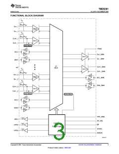
FUNCTIONAL BLOCK DIAGRAM
Vcc
RINT
RINT
Dx+_1
Dx–_1
TMDS Rx
w/ AEQ
Vcc
RINT
RINT
CLK+_1
CLK–_1
TMDS Rx
Clock Detect
VSadj
Tx
SCL1
Rx
Dx+_SINK
Dx–_SINK
TMDS Tx
Tx
SDA1
xx2
Rx
3:1
MUX
CLK+_SINK
CLK–_SINK
Vcc
TMDS Tx
RINT RINT
Dx+_3
Dx–_3
Rx
Tx
Rx
Tx
TMDS Rx
w/ AEQ
SCL_SINK
SDA_SINK
Vcc
RINT
RINT
CLK+_3
CLK–_3
TMDS Rx
Clock Detect
Clock Detect
Tx
Rx
Tx
SCL3
SDA3
Rx
HPD_SINK
I2C_SEL
LP
1 kW
1 kW
1 kW
HPD1
HPD2
HPD3
Local I2C
and
Control Logic
S1/SCL
S2/SDA
B0330-01
Copyright © 2008, Texas Instruments Incorporated
Submit Documentation Feedback
3
Product Folder Link(s) :TMDS361

 TI [ TEXAS INSTRUMENTS ]