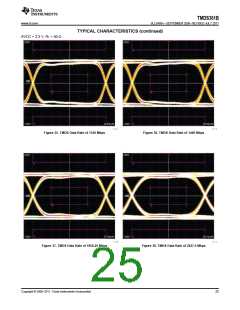
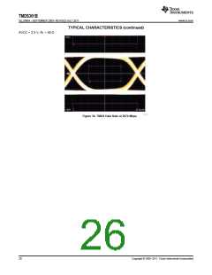
TMDS361B
www.ti.com
SLLS988A –SEPTEMBER 2009–REVISED JULY 2011
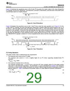
Figure 43 illustrates the waveforms seen on the R-side I2C-bus when the master writes to the slave through the
I2C repeater circuit of the TMDS361B. This looks like a normal I2C transmission, and the turnon and turnoff of the
acknowledge signals are slightly delayed.
9th Clock Pulse - Acknowledge From Slave
RSCL
RSDA
Figure 43. Bus-R Waveform
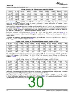
Figure 44 illustrates the waveforms seen on the T-side I2C-bus under the same operation as in Figure 43. On the
T-side of the I2C repeater, the clock and data lines would have a positive offset from ground equal to the VOL of
the driver T. After the eighth clock pulse, the data line is pulled to the VOL of the slave device, which is very close
to ground in this example. At the end of the acknowledge, the slave device releases and the bus level rises back
to the VOL set by the driver until the R-side rises above VCC/2, after which it continues to be high. It is important
to note that any arbitration or clock-stretching events require that the low level on the T-side bus at the input of
the TMDS361B I2C repeater is below 0.4 V to be recognized by the device and then transmitted to the R-side I2C
bus.
9th Clock Pulse - Acknowledge From Slave
TSCL
TSDA
V
Of Driver T
OL
V
Of Slave
OL
Figure 44. Bus-T Waveform
I2C Pullup Resistors
The pullup resistor value is determined by two requirements:
1. The maximum sink current of the I2C buffer:
The maximum sink current is 3 mA or slightly higher for an I2C driver supporting standard-mode I2C
operation.
Rup(min) = VDD / Isink
(1)
2. The maximum transition time on the bus:
The maximum transition time, T, of an I2C bus is set by an RC time constant, where R is the pullup resistor
value and C is the total load capacitance. The parameter, k, can be calculated from Equation 3 by solving for
t, the times at which certain voltage thresholds are reached. Different input threshold combinations introduce
different values of t. Table 4 summarizes the possible values of k under different threshold combinations.
t = k ´RC
(2)
V(t) = VDD 1- e-t/RC
(
)
(3)
Copyright © 2009–2011, Texas Instruments Incorporated
29

 TI [ TEXAS INSTRUMENTS ]