TMDS361B
www.ti.com
SLLS988A –SEPTEMBER 2009–REVISED JULY 2011
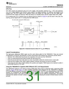
APPLICATION INFORMATION
Table 3. TMDS361B vs TMDS351 Pinout
PIN NUMBER I/O
TMDS351
TMDS361B
Pins 32 and 33
I
GPIO mode: S1 and S2 configured as
source selector pins
GPIO mode: S1 and S2 configured as source selector pins (same as
TMDS351)
I2C mode: S1 and S2 configured as SCL and SDA for local slave I2C
communication
Pin 34
I
EQ: TMDS input equalization control
select
I2C_SEL: GPIO / local I2C control select
EQ = High – 10-m 28 AWG HDMI cable
EQ = Low – HDMI 1.3 compliant cable
VDD: HPD/DDC power supply
I2C_SEL = High – Device is configured by GPIO logic.
I2C_SEL= Low – Device is configured by I2C logic.
LP: Low-power mode select bar
Pin 49
—
LP = High – Normal operational mode
LP = Low – Device goes into low-power state.
Based on the differences listed in Table 3, attention must be given to pin 34, which determines whether the
device uses I2C or GPIO control.
Supply Voltage
The TMDS361B is powered up with a single power source that is 3.3-V VCC for the TMDS circuitry for HPD,
DDC, and most of the control logic.
TMDS Input Fail-Safe
The TMDS361B incorporates clock-detect circuitry. If there is no valid TMDS clock from the connected HDMI/DVI
source, the TMDS361B does not switch on the terminations on the source-side data channels. Additionally, the
TMDS outputs are placed in the high-impedance state. This prevents the TMDS361B from turning on its outputs
if there is no valid incoming HDMI/DVI data.
TMDS Outputs
A 10% precision resistor, 4.02-kΩ, is recommended to control the output swing to the HDMI-supporting 800-mV
to 1200-mV range VOD(pp) (1000 mV typical). The TMDS outputs are high-impedance under standby-mode
operation, S1 = H and S2 = L.
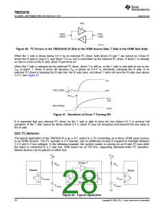
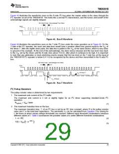
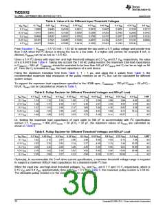
DDC I2C Function Description
The TMDS361B provides buffers on the DDC I2C lines on all three input ports. This section explains the
operation of the buffer. For representation, the source side of the TMDS361B is represented by RSCL/RSDA,
and the sink side is represented by TSCL/TSDA. The buffers on the RSCL/RSDA and TSCL/TSDA pins are 5-V
tolerant when the device is powered off and high-impedance under low supply voltage, 1.5 V or below. If the
device is powered up, the driver T (see Figure 40) is turned on or off depending on the corresponding R-side
voltage level.
When the R side is driven low, below 1.5 V, the corresponding T-side driver turns on and drives the T side down
to a low-level output voltage, VOL. The value of VOL and VIL on the T side or the sink side of the TMDS361B
switch depends on the output-voltage select (OVS) control settings. OVS control can be changed by the slave
I2C; see Table 8. When the OVS1 setting is selected, VOL is typically 0.7 V and VIL is typically 0.4 V. When the
OVS2 setting is selected, VOL is typically 0.6 V and VIL is typically 0.4 V. When the OVS3 setting (default) is
selected, VOL is typically 0.5 V and VIL is typically 0.3 V. VOL is always higher than the driver-R input threshold,
VIL on the T side or the sink side, preventing lockup of the repeater loop. The TMDS361B is targeted primarily as
a switch in the HDTV market and is expected to be a companion chip to an HDMI receiver; thus, the OVS control
has been provided on the sink side, so that the requirement of VIL to be less than 0.4 V can be met. The VOL
value can be selected to improve or optimize noise margins between VOL and VIL of the repeater itself or VIL of
some external device connected on the T side.
When the R side is pulled up, above 1.5 V, the T-side driver turns off and the T-side pin is high-impedance.
Copyright © 2009–2011, Texas Instruments Incorporated
27

 TI [ TEXAS INSTRUMENTS ]