TMDS361B
SLLS988A –SEPTEMBER 2009–REVISED JULY 2011
www.ti.com
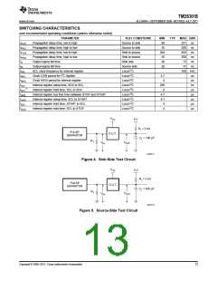
SWITCHING CHARACTERISTICS (continued)
over recommended operating conditions (unless otherwise noted)
PARAMETER
TEST CONDITIONS
MIN TYP(1)
MAX UNIT
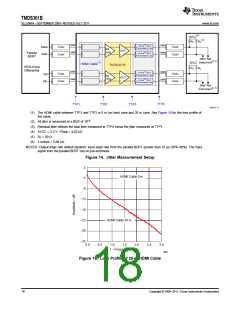
AVCC = 3.3 V, RT = 50 Ω, input TMDS clock
frequency = 225 MHz. See Figure 14for
measurement setup; residual jitter is the total
jitter measured at TTP4 minus the jitter
measured at TTP1. See Figure 15 for the loss
profile of the cable used for tJITC(PP)
tJITC(PP)
Peak-to-peak output residual clock jitter
54
84
ps
measurement. tJITC(PP) is measured at TMDS
differential clock signal crossing.
tCLK1
tCLK2
Valid clock-detect enable time
Invalid clock-detect disable time
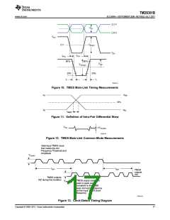
AVCC = 3.3 V, RT = 50 Ω, input TMDS clock
frequency = 300 MHz. See Figure 13.
300
500
500
800
ns
ns
AVCC = 3.3 V, RT = 50 Ω, input TMDS clock
frequency = 1 MHz. See Figure 13.
(4)
tSEL1
tSEL2
fCD
Port selection time (see
AVCC = 3.3 V, RT = 50 Ω
300
500
50
ns
ns
(5)
Port deselection time (see
Clock-detect frequency
)
AVCC = 3.3 V, RT = 50 Ω
40
AVCC = 3.3 V, RT = 50 Ω. See Figure 13.
25
300
MHz
(4) tSEL1 includes the time for the valid clock-detect enable time and tS1(HPD), because the tS1(HPD) event happens in parallel with tSEL1; thus,
the tSEL1 time is primarily the tCLK1 time.
(5) tSEL2 is primarily the tS2(HPD) time.
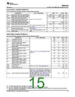
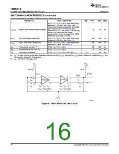
AVCC
VCC
50 W
50 W
50 W
50 W
0.5 pF
D+
D–
Y
Z
Driver
Receiver
VID
VD+
VY
VID = VD+ – VD–
VOD = VY – VZ
VD–
VZ
(VD+ + VD–
)
(VY + VZ)
2
VICM
=
VOC =
2
S0371-01
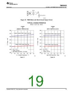
Figure 9. TMDS Main-Link Test Circuit
16
Copyright © 2009–2011, Texas Instruments Incorporated

 TI [ TEXAS INSTRUMENTS ]