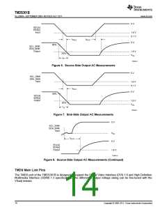
TMDS361B
SLLS988A –SEPTEMBER 2009–REVISED JULY 2011
www.ti.com
DEVICE POWER
The TMDS361B is designed to operate from a single 3.3-V supply voltage. The TMDS361B has three power
modes of operation. These three modes are referred to as normal mode, standby mode, and low-power mode.
Normal mode is designed to be used during typical operating conditions. In normal mode, the device is fully
functional and consumes the greatest amount of power.
Standby mode is designed to be used when reduced power is desired, but DDC and HPD communication must
be maintained. Standby mode can be enabled via the I2C interface (See Table 8 through Table 11) or GPIO
interface (See Table 1). In standby mode, the high-speed TMDS data and clock channels are disabled to reduce
power consumption. The internal I2C logic and DDC function normally. HPD[1:3] follow HPD_SINK.
Low-power mode is designed to consume the least possible amount of power while still applying 3.3 V to the
device. Low-power mode can be enabled by either the LP pin or by local I2C (See Table 8 through Table 11). In
low-power mode, all of the inputs and outputs are disabled with the exception of the internal I2C logic and LP pin.
The clock-detect feature in the TMDS361B provides an automatic power-management feature in normal mode. If
no valid TMDS clock is detected, the terminations on the input TMDS data lines are disconnected, and the TMDS
outputs are high-Z. As soon as a valid TMDS clock is detected, the terminations on the TMDS data lines are
connected, the TMDS outputs come out of high-Z, and the device is fully functional and consumes the greatest
amount of power.
ELECTRICAL CHARACTERISTICS
over recommended operating conditions (unless otherwise noted)
PARAMETER
TEST CONDITIONS
MIN
TYP MAX UNIT
LP = HIGH, TMDS: VID(pp) = 1200 mV, 3 Gbps TMDS data
pattern; HPD_SINK = HIGH, S1/S2 = LOW/LOW, LOW/HIGH,
HIGH/HIGH
ICC
Normal-mode supply current
170
216
mA
LP = HIGH, TMDS: VID(pp) = 1200 mV, 3 Gbps TMDS data
pattern; HPD_SINK = HIGH, S1 = HIGH, S2 = LOW
ISTBY
ISD
Standby supply current
Shutdown current
3
300
12
5.5
555
18
mA
μA
LP = LOW
Normal-mode supply current, with LP = HIGH, no TMDS input clock, HPD_SINK = HIGH,
no active TMDS input clock S1/S2 = LOW/LOW, LOW/HIGH, HIGH/HIGH
INCLK
mA
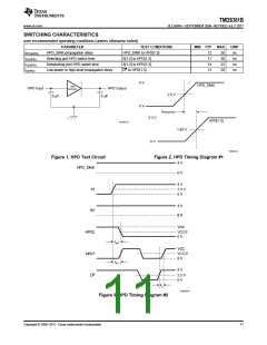
HOT-PLUG DETECT
The TMDS361B is designed to support the hot-plug indication to the input ports (HDMI/DVI sources connected to
the TMDS361B) via the HPD[1:3] output pins. The state of the hot-plug output of the selected source follows the
state of the hot-plug input (HPD_SINK input pin) from the sink side. The state of the hot-plug output for the
non-selected source goes low (See Table 1).
The maximum VOH of the HPD depends on VCC. It is recommended that if VOH greater than 3.6 V is needed on
HPD, then an external circuit can be used to drive VOH from the 5 V of the HDMI source (connected as shown in
Figure 45).
ELECTRICAL CHARACTERISTICS
over recommended operating conditions (unless otherwise noted)
PARAMETER
High-level output voltage
Low-level output voltage
High-level input current
Low-level input current
Output source impedance
TEST CONDITIONS
IOH = 100 μA
MIN TYP
MAX UNIT
VOH(HPD)
2
VCC
0.4
V
V
VOL(HPD)
IOL = 100 μA
0
IH
IL
VIH = 2 V, VCC = 3.6 V
VIL = 0.8 V, VCC = 3.6 V
–10
10
μA
μA
Ω
–10
10
RL
800 1000
1200
10
Copyright © 2009–2011, Texas Instruments Incorporated

 TI [ TEXAS INSTRUMENTS ]