TMDS261
www.ti.com ............................................................................................................................................................................................ SLLS953–DECEMBER 2008
V
VTdd
Rdd
Driver T
Driver R
R
RTup
Rup
Master
Slave
CSOURCE
CI
CO
Cslave
Cmedium
CCABLE
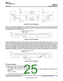
Figure 30. Typical Application
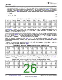
Figure 31 illustrates the waveforms seen on the R-side I2C-bus when the master writes to the slave through the
I2C repeater circuit of the TMDS261. This looks like a normal I2C transmission, and the turnon and turnoff of the
acknowledge signals are slightly delayed.
9th Clock Pulse - Acknowledge From Slave
RSCL
RSDA
Figure 31. Bus-R Waveform
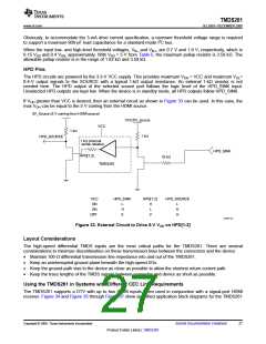
Figure 32 illustrates the waveforms seen on the T-side I2C-bus under the same operation as in Figure 31. On the
T-side of the I2C repeater, the clock and data lines would have a positive offset from ground equal to the VOL of
the driver T. After the 8th clock pulse, the data line is pulled to the VOL of the slave device, which is very close to
ground in this example. At the end of the acknowledge, the slave device releases and the bus level rises back to
the VOL set by the driver until the R-side rises above VCC/2, after which it continues to be high. It is important to
note that any arbitration or clock-stretching events require that the low level on the T-side bus at the input of the
TMDS261 I2C repeater is below 0.4 V to be recognized by the device and then transmitted to the R-side I2C bus.
9th Clock Pulse - Acknowledge From Slave
TSCL
TSDA
V
Of Driver T
OL
V
Of Slave
OL
Figure 32. Bus T Waveform
I2C Pullup Resistors
The pullup resistor value is determined by two requirements:
1. The maximum sink current of the I2C buffer:
The maximum sink current is 3 mA or slightly higher for an I2C driver supporting standard-mode I2C
operation.
Rup(min) = VDD/Isink
(1)
2. The maximum transition time on the bus:
Copyright © 2008, Texas Instruments Incorporated
Submit Documentation Feedback
25
Product Folder Link(s) :TMDS261

 TI [ TEXAS INSTRUMENTS ]